WELCOME To PROJECT CIRCUIT DESIGN

Search

Ahad, Mac 03, 2013

How to build Basic Inverter


Have you ever wanted to run a TV, stereo or other appliance while on the road or camping? Well, this inverter should solve that problem. It takes 12 VDC and steps it up to 120 VAC. The wattage depends on which tansistors you use for Q1 and Q2, as well as how "big" a transformer you use for T1. The inverter can be constructed to supply anywhere from 1 to 1000 (1 KW) watts.
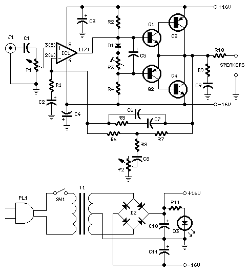
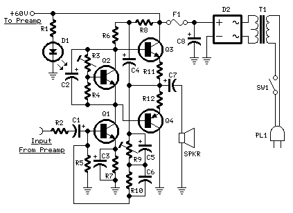
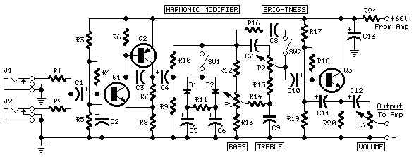
Circuit diagram

Parts:
C1, C2 68 uf, 25 V Tantalum Capacitor
R1, R2 10 Ohm, 5 Watt Resistor
R3, R4 180 Ohm, 1 Watt Resistor
D1, D2 HEP 154 Silicon Diode
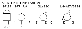
Q1, Q2 2N3055 NPN Transistor (see "Notes")
T1 24V, Center Tapped Transformer (see "Notes")
MISC Wire, Case, Receptical (For Output)
Notes:
1. Q1 and Q2, as well as T1, determine how much wattage the inverter can supply. With Q1,Q2=2N3055 and T1= 15 A, the inverter can supply about 300 watts. Larger transformers and more powerful transistors can be substituted for T1, Q1 and Q2 for more power.
2. The easiest and least expensive way to get a large T1 is to re-wind an old microwave transformer. These transformers are rated at about 1KW and are perfect. Go to a local TV repair shop and dig through the dumpster until you get the largest microwave you can find. The bigger the microwave the bigger transformer. Remove the transformer, being careful not to touch the large high voltage capacitor that might still be charged. If you want, you can test the transformer, but they are usually still good. Now, remove the old 2000 V secondary, being careful not to damage the primary. Leave the primary in tact. Now, wind on 12 turns of wire, twist a loop (center tap), and wind on 12 more turns. The guage of the wire will depend on how much current you plan to have the transformer supply. Enamel covered magnet wire works great for this. Now secure the windings with tape. Thats all there is to it. Remember to use high current transistors for Q1 and Q2. The 2N3055′s in the parts list can only handle 15 amps each.
3. Remember, when operating at high wattages, this circuit draws huge amounts of current. Don’t let your battery go dead
4. Since this project produces 120 VAC, you must include a fuse and build the project in a case.
5. You must use tantalum capacitors for C1 and C2. Regular electrolytics will overheat and explode. And yes, 68uF is the correct value. There are no substitutions.
6. This circuit can be tricky to get going. Differences in transformers, transistors, parts substitutions or anything else not on this page may cause it to not function.

How to build Variable 3 – 24 Volt / 3 Amp Power Supply


Description

This regulated power supply can be adjusted from 3 to 25 volts and is current limited to 2 amps as shown, but may be increased to 3 amps or more by selecting a smaller current sense resistor (0.3 ohm). The 2N3055 and 2N3053 transistors should be mounted on suitable heat sinks and the current sense resistor should be rated at 3 watts or more. Voltage regulation is controlled by 1/2 of a 1558 or 1458 op-amp. The 1458 may be substituted in the circuit below, but it is recommended the supply voltage to pin 8 be limited to 30 VDC, which can be accomplished by adding a 6.2 volt zener or 5.1 K resistor in series with pin 8. The maximum DC supply voltage for the 1458 and 1558 is 36 and 44 respectively. The power transformer should be capable of the desired current while maintaining an input voltage at least 4 volts higher than the desired output, but not exceeding the maximum supply voltage of the op-amp under minimal load conditions. The power transformer shown is a center tapped 25.2 volt AC / 2 amp unit that will provide regulated outputs of 24 volts at 0.7 amps, 15 volts at 2 amps, or 6 volts at 3 amps. The 3 amp output is obtained using the center tap of the transformer with the switch in the 18 volt position. All components should be available at Radio Shack with the exception of the 1558 op-amp.

Circuit diagram

Circuit diagram

How to build High Current Power Supply


Since my page was first posted, I have received a number of emails asking about a high current power supply. I looked around, but couldn’t find one that was suitable. So, I designed this. It is a linear supply, which might have a few of you rolling your eyes, but it takes very few parts, is simple to build and can supply huge currents.
Circuit diagram

Parts
R1 680 Ohm 1/4 Watt Resistor
C1 20,000 – 50,000uF 20-40 Volt Capacitor
C2, C3 100uF 50 Volt Capacitor
C4 0.1uF 50 Volt Capacitor
C5 0.01uF 50 Volt Capacitor
D1 Zener Diode (See Notes)
Q1 2N3055 Or Other (See Notes)
T1 Transformer (See Notes)
BR1 Bridge Rectifier (See Notes)
S1 SPST 250 VAC 10 A Switch
MISC Case, Line Cord, Heatsink For Q1, Binding Posts For Output
Notes
1. D1 should be rated at about one volt higher than then desired output of the supply. A half watt diode will do.
2. Q1 can be a transistor similar to the 2N3055. I chose the 2N3055 for it’s availability and power handling (150 watts).
3. T1 should be about 5 volts higher than the desired output of the supply, and rated for about one amp more of current. The voltage overhead is required by the regulator section. The extra current is to keep the transformer from over heating.
4. The choice of BR1 will depend on the voltage and current of your transformer. The rectifier should be rated for 50 volts more than the transformer, and 5 amps more than the transformer.
5. The value of R1 will be smaller when supplying high currents. Expiriment until you get what you need.
6. Heatsink and fans are absolutely necessary!


Most Wanted Diagrams:

  • how to build high power powersupply
  • how to build variable high current power supply

How to build Transformerless Power Supply

I have received a few emails asking for a transformerless power supply. Here is such a supply. This supply uses no heavy step down transformer and has an extremely low parts count. The circuit can be built very small and can supply small currents for small projects. The major downfall of this supply is that it is not isolated from the AC line and can only supply small currents.
Circuit diagram

Parts:
C1 0.39uF 250V Capacitor
C2 220uF 25V Electrolytic Capacitor
D1 1N4741 11V Zener Diode (See Notes)
BR1 1 Amp 200V Bridge Rectifier
MISC Line Cord, Board, Wire, Case
Notes:
1. The value of C1 can be increased to increase the amount of current the circuit can supply. With the values shown, the circuit can supply up to about 15mA. Remember to increase the size of C2 also.
2. A different value can be used for D1 to increase or decrease the voltage as needed.
3. Please note that this circuit is not isolated from 120VAC. Because of this, the circuit must be treated with caution and encosed at all times. Do not work on the circuit (or any other circuits attached to it) when it is plugged in.
4. You may want to add a resisor in series with C1 to limit current if the circuit is plugged in and the mains is at its full voltage.
5. If you are running the circuit from 220VAC, then use a capacitor rated at greater than 400V for C1.
6. If you want isolation from the AC line, you can connect up a small isolation transformer at the inputs of the circuit. Small 600ohm:600ohm audio transformers work nicely.

Most Wanted Diagrams:

12VDC Fluorescent Lamp Driver

A number of people have been unable to find the transformer needed for the Black Light project, so I looked around to see if I could find a fluorescent lamp driver that does not require any special components. I finally found one in Electronics Now. Here it is. It uses a normal 120 to 6V stepdown transformer in reverse to step 12V to about 350V to drive a lamp without the need to warm the filaments.
Circuit diagram

Parts:
C1 100uf 25V Electrolytic Capacitor
C2,C3 0.01uf 25V Ceramic Disc Capacitor
C4 0.01uf 1KV Ceramic Disc Capacitor
R1 1K 1/4W Resistor
R2 2.7K 1/4W Resistor
Q1 IRF510 MOSFET
U1 TLC555 Timer IC
T1 6V 300mA Transformer
LAMP 4W Fluorescent Lamp
MISC Board, Wire, Heatsink For Q1
Notes:
1. Q1 must be installed on a heat sink.
2. A 240V to 10V transformer will work better then the one in the parts list. The problem is that they are hard to find.
3. This circuit can give a nasty (but not too dangerous) shock. Be careful around the output leads.

Nite Rider Lights

Circuit diagram

The circuit is drawn with PCB 123 which you can download for free from http://www.pcb123.com
As a keen cyclist I am always looking for ways to be seen at night. I wanted something that was a novelty and would catch the motorists eye. So looking around at my fellow cyclists rear lights, I came up with the idea of 'NITE-RIDER'. NINE extra bright LED's running from left to right and right to left continuously. It could be constructed with red LEDs for use on the rear of the bike or white LED's for an extra eye catcher on the front of the bike.
All IC's are CMOS devices so that a 9V PP3 battery can be used, and the current drawn is very low so that it will last as long as possible.
Parts
1 555 timer IC4.
1 4027 flip flop IC1.
2 4017 Decade Counter IC2 and IC3.
3 4071 OR gate IC5, IC6 and IC7.
1 470 Ohm resistor 1/4 watt R3.
2 10K resistors 1/4 watt R1 and R2.
1 6.8UF Capasitor 16V C1.
9 Super brght LED's 1 to 9.
1 9V PP3 Battery.
1 single pole switch SW1.
1 Box.
How The Circuit Works.
IC4, C1, R1 and R2 are used for the clock pulse which is fed to both the counters IC2 and IC3 Pin 14.
IC1 is a Flip Flop and is used as a switch to enable ether IC2 or IC3 at pin 13.
IC7a detects when ether IC2 or IC3 has reached Q9 of the counter pin 11.
IC5, IC6 and IC7a protects the outputs of the counters IC2 and IC3 using OR gates which is then fed to the Anodes of the
LED's 1 to 9.

15W FM-transmitter

Warning: Take care with transmitter circuits. It is illegal in most countries to operate radio transmitters without a license
It was five years ago when I did an attempt to build my first fm-transmitter. It ended in a giant faillure. The only thing it did was interferring with our tv-set. Looking back it was due to the lack of information I had. A schematic was my only help. Now, five years later, I know a lot more about electro-technics. So I searched for a schematic of a stable, tested fm-transmitter with a far reach. I will put all information you'll have to know in my page. I made drawings to make things clearer. As said before: I'm still building it, so I will add information every time I made progress. It would be wise for you out there not to start building untill I'm ready and have tested it. It has been succesfully built before, but my succes will give you a double security. I remind you of the fact that I can also fail.

Intro
Building a good fm-transmitter(88-110Mhz) begins with getting a good schematic. You don't have to understand the precise working of the transmitter to build it. But some basic information won't harm. A transmitter alone is, as you probably know, is not enough to start your radio-station. In the simplest form you need 4 things. First an input device such as an amplifiler you also use with your home-stereo.
You can also use a walkman. Details about input-devices in the page: "Input". Second you need a regulated power-supply. In this case a 14-18 Volts/2,5-3,5 Ampere. One of the most influencial things you need is antenna and coax-cable. More about this later on. And finally the transmitter itself. You can devide the transmitter in two main parts: the oscilator and the amplifiler. The oscilator converts electric sound information into electromagnetic waves. The amplifiler gives these waves
a bigger amplitude.

Building
It's stable and has output of 15-18 watts. This enough to terrorize your wide surroundings at the fm-band.
The most often used technique to connect the components to each other is soldering them on a double sided copper-board. Another way is connecting the components floating. It is cheaper but very tricky. Below you see the copper-board layout(PCB). I designed it looking closely at the root scheme.


 now you have the surface to solder the electric components on.
Now a few basic rules for good soldering:
1. Use a special electronics-solderingrod with a slim top.
2. Use soldering-metal with an anti-oxidant-fluid core.
3. Don't heat the components! Heat the connection-point on your PCB.
4. Make sure that the surface is not too smooth.
5. Don't use too much metal.
6. Don't let the soldering metal form a bridge beetween two copper-surfaces.
7. If you're smart you start from the middle of your prepaired board.
In this way you'll have enough space.
Below the schematic. The yellow lines are pieces of copperboard that devide the transmitter in 3 parts. This is essential. Without them, internal interferrence will ruin your signal.


Parts

There are some components that need extra attention. Transistors usually have 3 or 4 different
wires comin' out. If you connect these wires in the wrong way the transmitter won't work. It may even explode. The picture below shows how to prevent from such an event.

You can find the numbers and letters back in the soldering schematic.
Coils also require extra attention. You can buy the coils trough ferrite in the shop, but the other ones have to be made yourself. Use 1mm AgCu wire. A coil like 7x/d=10mm/l=15mm, goes round 7 times, has an diameter of 10 millimeter and is long 15 millimeters. The best way to make a coil is to bend it around a pencil or other cilindrical shaped object tight. The diameter of the object is always d-coil minus 1 mm. In this case 9mm. As I said: bend the wire round (in this case 7times) with the revolves tight together. To get the desired length stretch the coil when still around the pencil
If you decide to build the transmitter and buy the parts, this list will be handy:
compon.doc
READ THIS E-MAIL I RECEIVED
Hello,
just to give some input: I have built the 15W FM transmitter you describe about 4.5 years ago.
The PCB lay out and component selection is still the same as it was then and after some modifications, I had an average output power of 16.8W @ 98.6 MHz (measured with Rhode and Schwarz equipement). You will need additional filtering on the power lines otherwise a stable power supply for the modulating circuit cannot be guaranteed. The legs of the modulating diode are, at best, kept long for extra capacitance. This to make sure you fall within the FM band because before I did that, I had
problems falling withing the 88-108 MHz. I was actually interfering with the police and fire brigade radio bands (Belgium). Of course, this is not the intention. I also advice you and readers to carefully check the orientation of the BLY88 because my professor blew one up due to lack of specification and inclarities in the datasheets (the actual pin out of the component changed a few years ago, resulting in a swapped emitter and collector - no good if you position it wrong!!! (the white cap flies of)). You will also need to play with the spacing between the windings of the different coils in order to get a good coupling between the different stages. I short circuited parts of the coils and made them smaller than specified to have near-optimal coupling. I also added extra ferrite bead coils for extra decoupling of the power lines, and used a very good shielding. Above 16.8W there is coupling (primarily through the air) between the output and the modulating/input stage and oscillation occurs. So for I have not found any other solution than lower the output power. Both extra decoupling
and extra shielding had no effect (my transmitter is built into a fully closed aluminium box with seperating plates that are fully connected to the case or ground plane on the PCB, except from where tracks run (0.5mm spacing provided)). Also, use a good heat sink for the last power stage!!!

THE High Quality Intercom

Description:
A very high quality intercom, which may also be used for room monitoring.


Circuit diagram


Notes:
This circuit consists of two identical intercom units. Each unit contains a power supply, microphone preamplifier, audio amplifier and a Push To Talk (PTT) relay circuit. Only 2 wires are required to connect the units together. Due to the low output impedance of the mic preamp, screened cable is not necessary and ordinary 2 core speaker cable, or bell wire may be used.
The schematic can be broken into 34 parts, power supply, mic preamp, audio amplifierand PTT circuit. The power supply is designed to be left on all the time, which is why no on / off switch is provided. A standard 12 V RMS secondary transformer of 12VA will power the unit. Fuses are provided at the primary input and also secondary, before the rectifier. The 1 A fuse needs to be a slow blow type as it has to handle the peak rectifier current as the power supply electrolytics charge from zero volts.
The microphone amplifier is a 2 transistor direct coupled amplifier. BC108B transistors will work equally well in place of the BC109C transistors. The microphone used is a 3 terminal electret condenser microphone insert. These are popular and require a small current to operate. The preamp is shown in my audio circuit section as well, but has a very high gain and low distortion. The last transistor is biased to around half the supply voltage; this provides the maximum overload margin for loud signals or loud voices. The gain may be adjusted with the 10k preset. Sensitivity is very high, and a ticking clock can easily be heard from the distant loudspeaker.
The amplifier is based on the popular National Semiconductor LM380. A 50 mV input is all thats required to deliver 2W RMS into an 8 ohm loudspeaker. The choice of loudspeaker determines overall sound quality. A small loudspeaker may not produce a lot of bass, I used an old 8 inch radio loudspeaker. The 4.7u capacitor at pin 1 of the LM380 helps filter out any mains hum on the power supply. This can be increased to a 10u capacitor for better power supply rejection ratio.
The push to talk (PTT) circuit is very simple. A SPDT relay is used to switch between mic preamplifier output or loudspeaker input. The normally closed contact is set so that each intercom unit is "listening". The non latching push button switch must be held to talk. The 100u capacitor across the relay has two functions. It prevents the relays back emf from destroying the semiconductors, and also delays the release of the relay. This delay is deliberate, and prevents any last word from being "chopped" off.
Setting Up and Testing:
This circuit does not include a "call" button. This is simply because it is designed to be left on all the time, someone speaking from one unit will be heard in the other, and vice versa. Setup is simple, set to volume to a comfortable level, and adjust the mic preset while speaking with "normal volume" from one meter away. You do not need to be in close contact with the microphone, it will pick up a conversation from anywhere in a room. If the units are a long way away, there is a tendency for the cable to pick up hum, or radio interference. There are various defenses against this. One way is to use a twisted pair cable, each successive turn cancels the interference from the turn before. Another method is to use a small capacitor of say 100n between the common terminal of each relay and ground. This shunts high frequency signals to earth. Another method is to use a low value resistor of about 1k. This will shunt interference and hum, but will shunt the speech signal as well. However as the output impedance of each mic preamp is low, and the speech signals are also low, this will have little effect on speech but reduce interference to an acceptable level.
IC Pinout:
The LM380 pinout viewed from above is shown below on the left. In the schematic, the LM380 has been represented as a triangle, the pins are shown on the right hand diagram. Pins marked "NC" have no connection and are not used.

PCB Layout:
Corey Rametta has kindly drafted a PCB layout for this project. First an oversized version to show component placement. Note the tracks on the bottom side, components on the top side.

Below is the actual size version shown track side.


500W low cost 12VDC to 220VAC inverter

Attention: This Circuit is using high voltage that is lethal. Please take appropriate precautions


 How to calculate transformer rating
The basic formula is P=VI and between input output of the transformer we have Power input = Power output
For example if we want a 220W output at 220V then we need 1A at the output. Then at the input we must have at least 18.3V at 12V because: 12V*18.3 = 220v*1
So you have to wind the step up transformer 12v to 220v but input winding must be capable to bear 20A.

60W Amplifier


Low-cut and Bass controls
Output power: 40W on 8 Ohm and 60W on 4 Ohm loads
Amplifier circuit diagram:

Amplifier parts:
R1 6K8 1W Resistor
R2,R4 470R 1/4W Resistors
R3 2K 1/2W Trimmer Cermet
R5,R6 4K7 1/2W Resistors
R7 220R 1/2W Resistor
R8 2K2 1/2W Resistor
R9 50K 1/2W Trimmer Cermet
R10 68K 1/4W Resistor
R11,R12 R47 4W Wirewound Resistors
C1,C2,C4,C5 47µF 63V Electrolytic Capacitors
C3 100µF 25V Electrolytic Capacitor
C6 33pF 63V Ceramic Capacitor
C7 1000µF 50V Electrolytic Capacitor
C8 2200µF 63V Electrolytic Capacitor (See Notes)
D1 LED Any type and color
D2 Diode bridge 200V 6A
Q1,Q2 BD139 80V 1.5A NPN Transistors
Q3 MJ11016 120V 30A NPN Darlington Transistor (See Notes)
Q4 MJ11015 120V 30A PNP Darlington Transistor (See Notes)
SW1 SPST Mains switch
F1 4A Fuse with socket
T1 220V Primary, 48-50V Secondary 75 to 150VA Mains transformer
PL1 Male Mains plug
SPKR One or more speakers wired in series or in parallel. Total resulting impedance: 8 or 4 Ohm. Minimum power handling: 75W
Preamplifier circuit diagram:

Preamplifier parts:
P1 10K Linear Potentiometer
P2 10K Log. Potentiometer
R1,R2 68K 1/4W Resistors
R3 680K 1/4W Resistor
R4 220K 1/4W Resistor
R5 33K 1/4W Resistor
R6 2K2 1/4W Resistor
R7 5K6 1/4W Resistor
R8,R18 330R 1/4W Resistors
R9 47K 1/4W Resistor
R10 18K 1/4W Resistor
R11 4K7 1/4W Resistor
R12 1K 1/4W Resistor
R13 1K5 1/4W Resistor
R14,R15,R16 100K 1/4W Resistors
R17 10K 1/4W Resistor
C1,C4,C8,C9,C10 10µF 63V Electrolytic Capacitors
C2 47µF 63V Electrolytic Capacitor
C3 47pF 63V Ceramic Capacitor
C5 220nF 63V Polyester Capacitor
C6 470nF 63V Polyester Capacitor
C7 100nF 63V Polyester Capacitor
C11 220µF 63V Electrolytic Capacitor
Q1,Q3 BC546 65V 100mA NPN Transistors
Q2 BC556 65V 100mA PNP Transistor
J1,J2 6.3mm. Mono Jack sockets
SW1 SPST Switch
Circuit description:
This design adopts a well established circuit topology for the power amplifier, using a single-rail supply of about 60V and capacitor-coupling for the speaker(s). The advantages for a guitar amplifier are the very simple circuitry, even for comparatively high power outputs, and a certain built-in degree of loudspeaker protection, due to capacitor C8, preventing the voltage supply to be conveyed into loudspeakers in case of output transistors' failure.
The preamp is powered by the same 60V rails as the power amplifier, allowing to implement a two-transistors gain-block capable of delivering about 20V RMS output. This provides a very high input overload capability.
Technical data:
Sensitivity:
70mV input for 40W 8 Ohm output
63mV input for 60W 4 Ohm output
Frequency response:
50Hz to 20KHz -0.5dB; -1.5dB @ 40Hz; -3.5dB @ 30Hz
Total harmonic distortion @ 1KHz and 8 Ohm load:
Below 0.1% up to 10W; 0.2% @ 30W
Total harmonic distortion @ 10KHz and 8 Ohm load:
Below 0.15% up to 10W; 0.3% @ 30W
Total harmonic distortion @ 1KHz and 4 Ohm load:
Below 0.18% up to 10W; 0.4% @ 60W
Total harmonic distortion @ 10KHz and 4 Ohm load:
Below 0.3% up to 10W; 0.6% @ 60W
Bass control:
Fully clockwise = +13.7dB @ 100Hz; -23dB @ 10KHz
Center position = -4.5dB @ 100Hz
Fully counterclockwise = -12.5dB @ 100Hz; +0.7dB @ 1KHz and 10KHz
Low-cut switch:
-1.5dB @ 300Hz; -2.5dB @ 200Hz; -4.4dB @ 100Hz; -10dB @ 50Hz
Notes:
The value listed for C8 is the minimum suggested value. A 3300µF capacitor or two 2200µF capacitors wired in parallel would be a better choice.
The Darlington transistor types listed could be too oversized for such a design. You can substitute them with MJ11014 (Q3) and MJ11013 (Q4) or TIP142 (Q3) and TIP147 (Q4).
T1 transformer can be also a 24 + 24V or 25 + 25V type (i.e. 48V or 50V center tapped). Obviously, the center-tap must be left unconnected.
SW1 switch inserts the Low-cut feature when open.
In all cases where Darlington transistors are used as the output devices it is essential that the sensing transistor (Q2) should be in as close thermal contact with the output transistors as possible. Therefore a TO126-case transistor type was chosen for easy bolting on the heatsink, very close to the output pair.
R9 must be trimmed in order to measure about half the voltage supply from the positive lead of C7 and ground. A better setting can be done using an oscilloscope, in order to obtain a symmetrical clipping of the output waveform at maximum output power.
To set quiescent current, remove temporarily the Fuse F1 and insert the probes of an Avo-meter in the two leads of the fuse holder.
Set the volume control to the minimum and Trimmer R3 to its minimum resistance.
Power-on the circuit and adjust R3 to read a current drawing of about 30 to 35mA.
Wait about 15 minutes, watch if the current is varying and readjust if necessary.

50W Amplifier

This is a handy, easy to build general purpose 50 watt amp. The amp has an input for a radio, TV, stereo or other line level device. It also has a phono input for a record player, guitar, microphone or other un-amplified source. With the addition of a low pass filter at the input, it makes a great amp for a small subwoofer.
circuit diagram

parts
R1 200 Ohm 1/4 W Resistor
R2 200K 1/4 W Resistor
R3 30K 1/4 W Resistor
R5 1K 1/4 W Resistor
R6 5K 1/4 W Resistor
R7,R10 1 Meg (5%) 1/2 W Resistor
R8,R9 0.4 Ohm 5 W Resistor
R11 10K Pot
R12,R13 51K 1/4 W Resistor
R14 47K 1/4 W Resistor
C1 100uF 35V Electrolytic Capacitor
C2 0.011uF Capacitor
C3 3750pF Capacitor
C4,C6 1000pF Capacitor
C5,C7,C8 0.001uF Capacitor
C9 50pF Capacitor
C10 0.3uF Capacitor
C11,C12 10,000uF 50V Electrolytic Capacitor
U1,U2 741 Op Amp
U3 ICL8063 Audio Amp Transister Driver thingy
Q1 2N3055 NPN Power Transistor
Q2 2N3791 PNP Power Transistor
notes
1. I know I skipped R4. That is not a problem :-)
2. Distortion is less than 0.1% up to 100HZ and increases to about 1% at 20kHz.
3. I haven't been able to find anyone who sells a suitable T1. You can always use two 24V 5A units in series. If you are building two amps (for stereo), then I would suggest using an old microwave transformer and rewinding it.
4. Q1 and Q2 will require heatsinks.

100W Amplifier


Circuit Description:
This is a 100 watt basic power amp that was designed to be (relatively) easy to build at a reasonable cost. It has better performance (read: musical quality) than the standard STK module amps that are used in practically every mass market stereo receiver manufactured today. When I originally built this thing, it was because I needed a 100 WPC amp and didn't want to spend any money. So I designed around parts I had in the shop.
The design is pretty much a standard one, and I'm sure there are commercial units out there that are similar. To my knowlwdge, it is not an exact copy of any commercial unit, nor am I aware of any patents on the topology. To experienced builders: I realize that many improvements and refinements can be made, but the idea was to keep it simple, and should be do-able by anyone who can make a circuit board and has the patience not to do a sloppy job.
The input stage is an LF351 op amp which provides most of the open loop gain as well as stabilizes the quiescent dc voltage. This feeds a level shift stage which references the voltage swing to the (-) rail. The transconductance stage is a darlington, to improve high-frerqency linearity. The 2SC2344 by itself has a rather large collector-base capacitance which is voltage dependent. The MPSA42 presents this with a low-z and has a C(ob) of only a few pf that is effectively swamped by the 33pF pole-splitting cap. The stage is supplied by the 2SA1011 active load (current source) which is about 20 ma. The current to the stage is limited by the 2N3094 to about 70 ma under worst case.
The output is a full complementary darlington with paralleled outputs. Although you could "get away with" only one if only 8 ohm easy-to-drive loads are used, this is not recommended. The use of parallel devices increases the ability to drive reactive loads (which can pull a significant current while the voltage waveform crosses zero and puts a high voltage and a high curent across the transistor simultaneously), gives the amp a higher damping factor, and reduces the maximum current each transistor has to supply to peaks (remember, the gain of a power transistor drops as the current increases).
Compensation is two-pole and one zero. The op-amp's pole and the pole generated by the 33pf cap and the 470 ohm bias resistor of the MPSA42 dominate. (the 33pF gets multiplied by the stage gain.) The 22 pf feedback capacitor provides lead compensation, and is taken from the output of the tranconductance stage rather than the output itself. In this way, the phase lag introduced by the output transistors is not seen by the high-frequency feedback. This intorduces a closed-loop pole which limits the high-frequency response. The two compensation capacitors must be type 1 creamic (NPO) or silver mica - with ZERO voltage coefficient.
The amp was designed to run 2 channels off a +/- 55 volt unregulated supply, reducing to +/- 48 volts under full load. It used a 40-0-40 volt, 5 amp toroid transformer, a bridge rectifier, and 10,000 uf of filter cap per side. If a standard EI transformer is used, a 6-amp rated unit should be used. With this power supply, it produces 100 watts continuous, both channels driven into 8 ohms resistive with no clipping. Dynamic headroom is about a db and a half. For more headroom, unloaded voltages to +/- 62 volts can be used with no circuit modification.
By the way, the schematic is in Postscript.
Limitations:
With no modifications the amp will drive 4-ohm speaker systems with no current limiting. The short-circuit current limit is set to about 4.5 amps peak, which will handle conventional speaker loads.(It will, of course, produce higher peak currents as the output voltage swing approaches the rail.) If you are going to be running some of those high-end speakers with impedance minima of half an ohm, or that stay reactive throughout most of the audio band ( ie, 0.5 +j3.2 ohms) you will probably already own a better amp than this. If the higher-power Motorola power transistors are used, it will drive a 2-ohm resistive load without problems (except heat).
I have never heard any slew-induced distortion on this amp with a CD player's band-limited (22KHz) signal. I suppose that real high-end freaks could pick it to pieces by hitting it with a TTL square wave mixed with a 19KHz stereo pilot tone and crank it up. I guarantee that there will be spurs all over the spectrum, but who listens to that?
Possible Modifications: (What if I want mo' power???)
The Toshiba output transistors (2SD424/2SB554 pair) shoud not be used with supply voltages above +/-60 volts. If you plan on cranking it up, use more in parallel or use the 250 watt Motorola pairs (MJ15024/MJ15025). If very low impedances are expected, raise the bias in the transconductance stage to give more base drive to the output darlingtons or add another current gain stage. Higher-Beta (and faster) power transistors can't handle reactive loads worth a crap. Don't substitute high-fT parts unless you are sure they have adequate second-breakdown capability.
The NE5532 op-amp can be used in the input stage. If more than one are used off the +/-15 volt shunt regulators (balanced ins, anti-slew Bessel filters, etc.) the 2.7K dropping resistors may need to be reduced to say, 1.8K ohm to maintain regulation. The 2.7K resistors will allow up to 4 LF351 type op amps off the regulator (I used a quad 347 for balanced inputs to avoid hum in a DJ setup).
Construction tips:
The output transistors and thermal compensator (2SC1567) will need to be mounted on a common heat sink - a finned unit measuring 5 in. high by 8 in. wide with 1.25 in fins should do nicely for one channel. (They look nice if you make the sides of the case out of them). Most normal applications won't require more cooling than this. The reason the 2SC1567 was chosen for the output bias regulator is because it is fully insulated - the ECG version will require additional mounting hardware. TO-3 hardware for the outputs is cheap and easy to get.
The driver transistors and voltage amps (2SC3344/2SA1011 pairs) will all require heatsinking as well. Individual TO-220 heat sinks on the circuit board will suffice - the voltage amps dissipate about 1.4 watts each. A common piece of 1/8 in. thick 1 in. wide X 4in. long angle aluminum will suffice for all 4 on each channel, but bear in mind that it must be oriented to take advantage of natural convection, and the transistors must be insualted.
Keep the imput grounds separate from everything else, and return them at ONE point. Failure to do so WILL result in high distortion (5% or so), or even oscillation.
The output stage bias should be set to about 25 milliamps in the output transistors. This value takes a while to stabilize, and you may have to monitor it over an hour or so during initial setup. To measure it, measure the voltage across the emitter resistor and use Ohm's law. This way, you can check the current sharing in the parallel output transistors at the same time and change them if there is a serious discrepancy. With parts of the same date code, they should not be off by more than 10% after it has warmed up. Higher output stage biases can be used, but it takes more care in setting it. If you want an idle current of more than 50 milliamps per side, increase the value of the emitter resistors.
Initial Checkout:
DO NOT just plug something like this in! A seemingly insignificant error can set your house on fire! (As well as blow out $30 worth of transistors in a microsecond.) A variac will work in theory, but the amp may latch to the rail if the supply drops too low. I suggest the use of a ballast resistor - a 60 to 100 watt light bulb in series with the AC mains. You get a bright flash when the caps charge, and then it goes (almost) out as the idling supply current reaches its nominal low value. The amplifier will then work normally at low volumes. If the amp draws too much current for whatever reason, the lightbulb will glow brightly, increase resistance, and limit the power to the circuit. Usually, there will either be a mis-wire (use your DMM) or oscillation (will show up on a scope or RF power measuring device). If the bulb goes dim-bright-dim-bright... then the amp is marginally stable and the grounding layout should be checked. Compensation capacitor values may need to be adjusted if any significant changes were made. Mine is stable the way it is.
Additional Notes:
The schematic is in postcript, so it should just be able to be printed out. The emitters of the transistors are labelled by an "e". I was too lazy to put arrows on the transistor symbols - and I've been using it that way for over a year now.
Trouble finding parts? MCM (1-800-543-4330) has all the transistors. Total cost for a stereo version should be between $150 and $250, depending on what kind of bargains you can find on the case, transformer, and heatsinks. If you have to pay "list" for everything, it will likely cost about $1000 to build.
The information included herin is provided as-is, with no warranties express or implied. No resposibility on the part of the author is assumed for the technical accuracy of the information given herein or the use or mis-use of said information.
The equipment described in this article was designed, fabricated, and tested on my own personal time using my own personal resources.


Click HERE to get the postscript circuit diagram.
Click HERE to get the pdf circuit diagram.

10W Mini Audio Amplifier

finished device

Componets Layout

PCB

Componets List
R1 : 6 Ohm
R2 : 220 Ohm
R3 : nothing
R4 : 10 KOhm pontesiometer
C1 : 2200 uF / 25V
C2 : 470 uF / 16V
C3 : 470 nF / 63V
C4 : 100 nF
C5 : nothing
C6 : nothing
IC1 : TDA 2003

Subwoofer Power Amplifier


he acoustic spectrum is extended by very low frequencies 20Iz and reaches as the 20000Iz in high frequencies. In the low frequencies is degraded the sense of direction. This reason us leads to the utilization speaker for the attribution of very low frequencies. The manufacture that to you we propose distinguishes these frequencies, in order to him we lead to the corresponding amplifier. The acoustic filters are met in various points in the sound systems. The knownest application they are the filters baxandal for regulating tone low and high frequencies and filters crossover where the acoustic region is separated in subareas, in order to it leads the corresponding loudspeakers. The application that to you we propose is a simple filter of region that limits the acoustic region (20-20000Hz) in the region 20-100Hz.
With the manufacture that to you we propose you can make a active filter in order to you lead a loudspeaker of very low frequencies. With this you will place one bigger speaker between the HIFI speakers of you. In order to you have a complete picture of sound you will need also the corresponding amplifier. In the entry of circuit you will connect the two exits of preamplifier or the exit of line of some preamplifier. The circuit of manufacture allocates a exit in order to is led means of circuit of force subwoofer. If for some reason you do not have space in order to you place the third speaker in space of hearing, then you can select smaller speaker. The output will depend from the type of music that you hear. If in deed you have space, then after you make a filter and remain thanked, you can him recommend in your friends or still make other same for your friends.


In the form it appears the theoretical circuit of filter. In first glance we see three different circuits that are mainly manufactured round two operational amplifiers. This circuits constitute mixed, amplifier with variable aid and a variable filter. The manufacture end needs a circuit of catering with operational tendency of catering equal with ±12. the operational amplifiers that constitute the active elements for this circuits of are double operational type as the TL082 and NE5532. The operational these amplifiers belong in a family provided with transistor of effect of field IFET in their entries. Each member of family allocates in their circuit bipolar transistor and effect of field. This circuits can function in his high tendency, because that they use transistor of high tendency. Also they have high honor of rhythm of elevation (slew rate), low current of polarization for the entries and are influenced little by the temperature. The operational these amplifiers have breadth of area unity gain bandwidth 3MHz. A other important element for their choice is the big reject of noise, when this exists in the line of catering.
The price of reject is bigger than 80dB, their consumption is small, from 11 until 3 mA. They are internally sold in nutshell with eight pins and allocate two operational amplifiers, In the same line in nutshell 14 pins they incorporate four operational, In the trade they are sold with code TL074, TL084 and TL064, In nutshell with eight pins they are sold operational amplifiers TL061 TL071 kajTL081. In the manufacture we used the TL082 that has two operational. First operational from the TL082 it works as amplifier and mixed for the two channels, In his negative entry he exists one small mixed with two resistances. A potentiometer in this rung determines the aid of circuit. In the point this left winger and the right channel of preamplifier they are added means of two resistances. En continuity the operational strengthens signal with aid made dependent from the price that has the potentiometer.
The place of runner is proportional with the aid of circuit. The second operational amplifier is the filter of manufacture. The filter of is acoustic frequency of second class and he is made with the materials that are round the operational amplifier. The filter of is low passage with variable frequency of cutting off. This frequency can be altered and take prices from very low frequency the 30Hz or still exceed 150Hz. The frequency of cutting off of filter depends from the prices that have the elements of circuit. Altering the values of elements we can have frequency of cutting off 150Iz, 130Iz, J00Iz, 7Ïz, 6Íz even 3Íz, this prices they can be achieved with the simple rotation of double potentiometer. The circuit of filter has been made around one operational' that it has completed TL082 that is double operational amplifier. In the exit of filter we will link the plug of expense where is connected the amplifier. In the exit of circuit is presented, the limited as for the breadth of frequencies, signal that we apply in the entry of circuit.
Manufacture
Parts
R1 = 39 Kohm
R2 = 39 Kohm
R3 = 47 Kohm
R4 = 10 Ohm
R5 = 22 Kohm
R6 = 4,7 Kohm
R7 = 22 Kohm
R8 = 4,7 Kohm
R9 = 10 Ohm
R10 = 220 Ohm
C1 = 39 pF
C2 = 0.1 uF
C3 = 0.1 uF
C4 = 0.2 uF
C5 = 0.4 uF
C6 = 0.1 uF
C7 = 0.1 uF
IC1 = TL064
In order to you make the manufacture you will need printed that appears in the form. In this you will place the materials according to the following form. The materials are enough also easy can become certain errors. With few attention however you can him avoid. If they are presented difference malfunctions, you check carefully the circuit. The circuit, as we said, is filter and it should they are used materially good precision and quality, particularly for the capacitors. The capacitors of filters will have tolerance 5%. Of course, the manufacture will also work with material of lower quality, the trial of manufacture can become with acoustic signal of generator We apply the generator in the entry of manufacture and we measure with a voltmeter the tendency in the exit of filter. If we alter the potentiometer and are altered the tendency, then all have well.

2N3055 Power Amplifier


Simple and low cost. The optimal supply voltage is around 50V, but this amp work from 30 to 60V. The maximal input voltage is around 0.8 - 1V. As you can see, in this design the components have a big tolerance, so you can build it almost of the components, which you find at home. The and transistors can be any NPN type power transistor, but do not use Darlington types... The output power is around 60W.
Some comments:
- capacitor C1 regulates the low frequencies (bass), as the capacitance grows, the low frequncies are getting louder.
- capacitor C2 regulates the higher frequencies (treble), as the capacitance grows, the higher frequencies are getting quiter.
- this is a class B amplifier, this means, that a current must flow through the end transistors, even if there is no signal on the input. This current can be regulated with the 500ohm; trimmer resistor. As this current incrases, the sound of the amplifier gets better, but the end transistors are more heating. But if this current decrases, the transistors are not heating so much, but the sound gets worse...


It's well known that many animals are particularly sensitive to high-frequency sounds that humans can't hear. Many commercial pest repellers based on this principle are available, most of them operating in the range of 30 to 50 kHz. My aim was, however, to design a slightly different and somewhat more powerful audio frequency/ultrasonic sound generator that could be used to train dogs. Just imagine the possibilities - you could make your pet think twice before barking again in the middle of the night or even subdue hostile dogs (and I guess burglars would love that!). From what I've read, dogs and other mammals of similar size behave much differently than insects. They tend to respond best to frequencies between 15 and 25 kHz and the older ones are less susceptible to higher tones. This means that an ordinary pest repeller won't work simply because dogs can't hear it. Therefore, I decided to construct a new circuit (based on the venerable 555, of course) with a variable pitch and a relatively loud 82 dB miniature piezo beeper. The circuit is very simple and can be easily assembled in half an hour. Most of the components are not really critical, but you should keep in mind that other values will probably change the operating frequency. Potentiometer determines the pitch: higher resistance means lower frequency. Since different dogs react to different frequencies, you'll probably have to experiment a bit to get the most out of this tiny circuit. The circuit is shown below:
Circuit diagram

Despite the simplicity of the circuit, there is one little thing. The 10nF (.01) capacitor is critical as it, too, determines the frequency. Most ceramic caps are highly unstable and 20% tolerance is not unusual at all. Higher capacitance means lower frequency and vice-versa. For proper alignment and adjustment, an oscilloscope would be necessary. Since I don't have one, I used Winscope. Although it's limited to only 22 kHz, that's just enough to see how this circuit works. There is no need to etch a PCB for this project, perf board will do. Test the circuit to see how it responds at different frequencies. A 4k7 potentiometer in conjunction with a 10nF (or slightly bigger) capacitor gives some 11 to 22kHz, which should do just fine. Install the circuit in a small plastic box and if you want to, you can add a LED pilot light. Power consumption is very small and a 9V battery should last a long time. Possible further experimentation: I'm working on an amplified version of the whistle to get a louder beep. All attempts so far haven't been successful as high frequency performance tends to drop dramatically with the 555. Perhaps I could use a frequency doubler circuit - I just don't know and I've run out of ideas. One other slightly more advanced project could be a simple "anti-bark" device with a sound-triggered (clap) switch that sets off the ultrasonic buzzer as soon as your dog starts to bark.

Insect Repellant


Circuit diagram
Notes:
Repell those repugnent insects from your Garden this Summer with this insect repellant circuit. Designed by Graham Maynard the circuitry consists of a phase locked loop (CMOS 4047) wired as a 22KHz oscillator. The output is amplified by a pair of complimentary output transistors and drives a Motorola 3.25 inch Piezo. Current drain is around 120mA so an external power supply is recommended.
The piezo used was a standard 85mm square Motorola Horn, Maplin part number WF09K or WF55K. These are rated +/-3dB to 28kHz.

20Wpp Audio Amplifier with Bass


Audio circuit diagram

Parts:
P1 22K Log.Potentiometer (Dual-gang for stereo)
P2 100K Log.Potentiometer (Dual-gang for stereo)
R1 820R 1/4W Resistor
R2,R4,R8 4K7 1/4W Resistors
R3 500R 1/2W Trimmer Cermet
R5 82K 1/4W Resistor
R6,R7 47K 1/4W Resistors
R9 10R 1/2W Resistor
R10 R22 4W Resistor (wirewound)
C1,C8 470nF 63V Polyester Capacitor
C2,C5 100uF 25V Electrolytic Capacitors
C3,C4 470uF 25V Electrolytic Capacitors
C6 47pF 63V Ceramic or Polystyrene Capacitor
C7 10nF 63V Polyester Capacitor
C9 100nF 63V Polyester Capacitor
D1 1N4148 75V 150mA Diode

IC1 NE5532 Low noise Dual Op-amp

Q1 BC547B 45V 100mA NPN Transistor
Q2 BC557B 45V 100mA PNP Transistor
Q3 TIP42A 60V 6A PNP Transistor
Q4 TIP41A 60V 6A NPN Transistor
J1 RCA audio input socket


Power supply parts:
R11 1K5 1/4W Resistor
C10,C11 4700uF 25V Electrolytic Capacitors
D2 100V 4A Diode bridge
D3 5mm. Red LED
T1 220V Primary, 12 + 12V Secondary 24-30VA Mains transformer
PL1 Male Mains plug
SW1 SPST Mains switch
Comments:
This design is based on the 18 Watt Audio Amplifier, and was developed mainly to satisfy the requests of correspondents unable to locate the TLE2141C chip. It uses the widespread NE5532 Dual IC but, obviously, its power output will be comprised in the 9.5 - 11.5W range, as the supply rails cannot exceed ±18V.
As amplifiers of this kind are frequently used to drive small loudspeaker cabinets, the bass frequency range is rather sacrificed. Therefore a bass-boost control was inserted in the feedback loop of the amplifier, in order to overcome this problem without quality losses. The bass lift curve can reach a maximum of +16.4dB @ 50Hz. In any case, even when the bass control is rotated fully counterclockwise, the amplifier frequency response shows a gentle raising curve: +0.8dB @ 400Hz, +4.7dB @ 100Hz and +6dB @ 50Hz (referred to 1KHz).
Notes:
Can be directly connected to CD players, tuners and tape recorders.
Schematic shows left channel only, but C3, C4, IC1 and the power supply are common to both channels.
Numbers in parentheses show IC1 right channel pin connections.
A log type for P2 ensures a more linear regulation of bass-boost.
Don't exceed 18 + 18V supply.
Q3 and Q4 must be mounted on heatsink.
D1 must be in thermal contact with Q1.
Quiescent current (best measured with an Avo-meter in series with Q3 Emitter) is not critical.
Set the volume control to the minimum and R3 to its minimum resistance.
Power-on the circuit and adjust R3 to read a current drawing of about 20 to 25mA.
Wait about 15 minutes, watch if the current is varying and readjust if necessary.
A correct grounding is very important to eliminate hum and ground loops. Connect in the same point the ground sides of J1, P1, C2, C3 &C4. Connect C9 at the output ground.
Then connect separately the input and output grounds at the power supply ground.
Technical data:
Output power: 10 Watt RMS @ 8 Ohm (1KHz sinewave)
Sensitivity: 115 to 180mV input for 10W output (depending on P2 control position)
Frequency response: See Comments above
Total harmonic distortion @ 1KHz: 0.1W 0.009% 1W 0.004% 10W 0.005%
Total harmonic distortion @ 100Hz: 0.1W 0.009% 1W 0.007% 10W 0.012%
Total harmonic distortion @10KHz: 0.1W 0.056% 1W 0.01% 10W 0.018%
Total harmonic distortion @ 100Hz and full boost: 1W 0.015% 10W 0.03%
Max. bass-boost referred to 1KHz: 400Hz = +5dB; 200Hz = +7.3dB; 100Hz = +12dB; 50Hz = +16.4dB; 30Hz = +13.3dB
Unconditionally stable on capacitive loads

60W Guitar Amplifier


Bass, Treble, Harmonic modifier and Brightness controls

Output power: 40W on 8 Ohm and 60W on 4 Ohm loads
Amplifier circuit diagram:

Amplifier parts:
R1 6K8 1W Resistor
R2,R4 470R 1/4W Resistors
R3 2K 1/2W Trimmer Cermet
R5,R6 4K7 1/2W Resistors
R7 220R 1/2W Resistor
R8 2K2 1/2W Resistor
R9 50K 1/2W Trimmer Cermet
R10 68K 1/4W Resistor
R11,R12 R47 4W Wirewound Resistors
C1,C2,C4,C5 47µF 63V Electrolytic Capacitors
C3 100µF 25V Electrolytic Capacitor
C6 33pF 63V Ceramic Capacitor
C7 1000µF 50V Electrolytic Capacitor
C8 2200µF 63V Electrolytic Capacitor (See Notes)
D1 LED Any type and color
D2 Diode bridge 200V 6A
Q1,Q2 BD139 80V 1.5A NPN Transistors
Q3 MJ11016 120V 30A NPN Darlington Transistor (See Notes)
Q4 MJ11015 120V 30A PNP Darlington Transistor (See Notes)
SW1 SPST Mains switch
F1 4A Fuse with socket
T1 220V Primary, 48-50V Secondary 75 to 150VA Mains transformer (See Notes)
PL1 Male Mains plug
SPKR One or more speakers wired in series or in parallel. Total resulting impedance: 8 or 4 Ohm. Minimum power handling: 75W
Preamplifier circuit diagram:

Preamplifier parts:
P1,P2 10K Linear Potentiometers
P3 10K Log. Potentiometer
R1,R2 68K 1/4W Resistors
R3 680K 1/4W Resistor
R4 220K 1/4W Resistor
R5 33K 1/4W Resistor
R6,R16 2K2 1/4W Resistors
R7 5K6 1/4W Resistor
R8,R21 330R 1/4W Resistors
R9 47K 1/4W Resistor
R10 470R 1/4W Resistor
R11 4K7 1/4W Resistor
R12,R20 10K 1/4W Resistors
R13 100R 1/4W Resistor
R14,R15 47R 1/4W Resistors
R17,R18,R19 100K 1/4W Resistors
C1,C4,C5,C6 10µF 63V Electrolytic Capacitors
C2 47µF 63V Electrolytic Capacitor
C3 47pF 63V Ceramic Capacitor
C7 15nF 63V Polyester Capacitor
C8 22nF 63V Polyester Capacitor
C9 470nF 63V Polyester Capacitor
C10,C11,C12 10µF 63V Electrolytic Capacitors
C13 220µF 63V Electrolytic Capacitor
D1,D2 BAT46 100V 150mA Schottky-barrier Diodes (see Notes)
Q1,Q3 BC546 65V 100mA NPN Transistors
Q2 BC556 65V 100mA PNP Transistor
J1,J2 6.3mm. Mono Jack sockets
SW1,SW2 SPST Switches
Circuit description:
This design adopts a well established circuit topology for the power amplifier, using a single-rail supply of about 60V and capacitor-coupling for the speaker(s). The advantages for a guitar amplifier are the very simple circuitry, even for comparatively high power outputs, and a certain built-in degree of loudspeaker protection, due to capacitor C8, preventing the voltage supply to be conveyed into loudspeakers in case of output transistors' failure.
The preamp is powered by the same 60V rails as the power amplifier, allowing to implement a two-transistors gain-block capable of delivering about 20V RMS output. This provides a very high input overload capability.
Technical data:
Sensitivity:
35mV input for 40W 8 Ohm output
42mV input for 60W 4 Ohm output
Frequency response:
50Hz to 20KHz -0.5dB; -1.5dB @ 40Hz; -3.5dB @ 30Hz
Total harmonic distortion @ 1KHz and 8 Ohm load:
Below 0.1% up to 10W; 0.2% @ 30W
Total harmonic distortion @ 10KHz and 8 Ohm load:
Below 0.15% up to 10W; 0.3% @ 30W
Total harmonic distortion @ 1KHz and 4 Ohm load:
Below 0.18% up to 10W; 0.4% @ 60W
Total harmonic distortion @ 10KHz and 4 Ohm load:
Below 0.3% up to 10W; 0.6% @ 60W
Treble control:
+9 / -16dB @ 1KHz; +12 / -24dB @ 10KHz
Brightness control:
+6.5dB @ 500Hz; +7dB @ 1KHz; +8.5dB @ 10KHz
Bass control:
-17.5dB @ 100Hz; -26dB @ 50Hz; -28dB @ 40Hz
Notes:
The value listed for C8 is the minimum suggested value. A 3300µF capacitor or two 2200µF capacitors wired in parallel would be a better choice.
The Darlington transistor types listed could be too over sized for such a design. You can substitute them with MJ11014 (Q3) and MJ11013 (Q4) or TIP142 (Q3) and TIP147 (Q4).
T1 transformer can be also a 24 + 24V or 25 + 25V type (i.e. 48V or 50V center tapped). Obviously, the center-tap must be left unconnected.
D1 and D2 can be any Schottky-barrier diode types. With these devices, the harmonic modifier operation will be hard. Using for D1 and D2 two common 1N4148 silicon diodes, the harmonic modifier operation will be softer.
In all cases where Darlington transistors are used as the output devices it is essential that the sensing transistor (Q2) should be in as close thermal contact with the output transistors as possible. Therefore a TO126-case transistor type was chosen for easy bolting on the heatsink, very close to the output pair.
R9 must be trimmed in order to measure about half the voltage supply from the positive lead of C7 and ground. A better setting can be done using an oscilloscope, in order to obtain a symmetrical clipping of the output waveform at maximum output power.
To set quiescent current, remove temporarily the Fuse F1 and insert the probes of an Avo-meter in the two leads of the fuse holder.
Set the volume control to the minimum and Trimmer R3 to its minimum resistance.
Power-on the circuit and adjust R3 to read a current drawing of about 30 to 35mA.
Wait about 15 minutes, watch if the current is varying and readjust if necessary.

Sabtu, Mac 02, 2013

LM555 Timer Circuit


LIST


Resistors (all 0.12 watt, ± 5% Carbon)

R1= 1 KΩ
R2 = 150 KΩ
R3, R4 = 330 Ω


Capacitor
C1 = 10 µF/16 V

Semiconductors

D1 and D2 = Green and Red LED Respectively
Miscellaneous
8 pin IC Base

SW1 = Push to on switch


Timer IC NE555 is very popular and most usable in electronics circuit. Timer IC NE555 is also called Ideal IC because it is multipurpose, low power consumption, small size and durable. Mostly there is fault in circuit but our first doubt is on IC because IC is the combination of many more components or IC itself is a combination of circuit. Here is the simple but effective IC tester circuit which check IC NE555 whether it have fault or not.


Working of the circuit timer IC NE555 

In the circuit IC NE555 itself is used as astable multivibrator mode. Switch SW1 is pushed for power supplies which charge the capacitor C1 through resistor R1 and variable resistor R­2 which trigger IC and high output is obtained from pin no 3 which glow LED D2 (LED D1 off). Similarly when capacitor is discharged the output become low and LED D1 glow (LED D2 off). The on and off of LED in sequence is in practice until power supply, this mean there is no fault in IC. But if the LED is not glow or on and off in sequence then there is fault in IC.


1. Data sheets NE/SA/SE555/SE555C

2. Advance used NE555

     2.1


      2.2  Driver LED circuit for Indicator using


     2.3 Night Rider


       2.4  More


Jumaat, Mac 01, 2013

Traffic Light Control Circuit


Traffic Light Control Circuit


20 Output Sequencing Circuit

  This page features a circuit that has twenty open collector outputs that turn on one at a time in a continuous, unidirectional loop sequence. The circuit uses the 74LSxx family of TTL integrated logic devices. The circuits are designed to drive light emitting diodes or low current, low voltage incandescent lights but can also drive other loads of up to 80 milliamps.
  As logic circuits go, the 20 Step circuit is fairly simple but due to the nature of the TTL Logic devices used, care must be taken when wiring these circuits. Simply put; The neater the wiring the better.
  NOTE: The 20 Step Circuit does not work in circuit simulation programs. The likely cause is that this circuit uses input states that force the outputs of the 74LS145 drivers to be turned off. These states would normally not be used with these devices and are probably not programmed into the simulator's software.
  If you would like to make use of these circuits, take the time to find and read at least the first 2 pages of the manufactures datasheets for the integrated circuits. Using Google,search for "74ls(part number)" in the first box and "PDF" in the second box on the advanced search page.

A printed circuit board and parts are available for this circuit.


20 Output Sequencing Circuit

  The following schematic is for the 20 Output Sequencing Circuit on the circuitboard shown above.

Basic Circuit Operation

  •   The circuit is stepped through the sequence by an adjustable LM555 astable oscillator.
  •   The Oscillators output is divided by a 74LS90 divider into a 10 step BCD weighted output.
  •   The BCD output then drives two 74LS145 - 1 of 10 decoders (See Notes) that are used to produce a 1 of 20 step output sequence.

Notes

  •   The circuit does not drive the 74LS145's directly but uses a 74LS107 JK Flip-Flop and four 74LS32 dual input OR gates to control to the inputs to the two 74LS145 output drivers. The 74LS107 and 74LS32 are used to create disallowed states in the output drivers alternately. The disallowed states prevent any of the ten outputs on that particular device from being turned ON while the other 74LS145 is in counting to ten.
  •   This produces a system where only one of the 74LS145's is able to produce a LOW output state at a time. In essence the circuit counts to 10 twice in succession rather than counting to 20 in a single cycle.
  •   This is an unusual logic scheme but it allows the circuit to make economical use of the open collector outputs of the 74LS145s decoder/drivers rather using output buffer ICs that are driven by 74LS138 logic devices which have eight steps.
  •   The TTL family devices used in the circuit require a regulated 5 volt supply and draw approximately 60 miliamps.
  •   The outputs of the 74LS145's can be supplied from up to 15 Volts with a maximum current of 80 milliamps.
  •   The circuit above is shown in a continuous running mode. The circuit can also be stopped and reset externally as shown in later diagrams.

74LS145 Equivalent Output Circuit


Parts List

  The following is a parts list for use with the 20 Output Sequencing Circuit. Mouser Electronics part numbers are shown but the parts may be available from other sources as well. Suppliers that handle 'NTE' components should be able to get the ICs.


20 Output Circuit - PCB Parts Placement Diagram

Save and print this diagram to aid in assembling the circuitboard.

Circuit Board Parts Placement Diagram

+++++++++++++++++++++++++++++++++++++++++++++++++++++++++

20 Output Sequencing Circuit PCB And Parts


20 Output Sequencing Circuit PCB - Assembled Example

  The printed circuit board is 2.9 inches square and has been commercially made.
  The picture shows the circuit board wired for continuous running for the Traffic Light Control circuit. Other modes of operation will be shown in diagrams lower on the page.


The ICs for the 20 Step circuit board are not available at this time.

  •   The price of the 20 Output Sequencing Circuit circuit boards is: $12.50 US each plus postage. (Each additional board is 12.00 dollars.)  NOTE: Some of the components supplied with the kit are not from Mouser Electronics.
      If you are interested in printed circuit boards and parts for this circuit, please send an email to the following address: rpaisley4@cogeco.ca
      Your message will be answered as soon as possible.


    20 Step LED Circuit

      The next diagram shows a simple 20 LED driver circuit. Only one current limiting resistor is needed as only one LED can be on at a time.

    Single Traffic Light Control Circuit

      If you only need to control a one set of traffic lights for a display, refer to the Single Traffic Light Driver Circuit page at this site.


    20 Step Traffic Light Schematic

      The next diagram shows the output of the 20 Step circuit being used to control a set of traffic Lights.


      The next circuit has the same function as the one above but can drive higher current lamps such as the #1157 automotive bulb.


    Manual Control Circuits

      The following circuits allow the 20 Step circuit to be controlled manually and to have a shortened sequence length.

    Stop, Start and Reset

      The next diagram and image shows external controls that can be used to manually Start, Stop and Reset the circuit. When the circuit is reset the 555 clock will stop and the number 1 output will go to a LOW state.
      If the RESET terminal is held LOW the circuit will run continuously. The RUN terminal has limitations (CLOCK input of the 74LS107) that are explained on the data sheet for the device.

      The next photo shows the location of the RUN and RESET connections on the circuit board. A jumper normally between the RUN connection and the circuit common must be removed first. Also shown are 5 volt and common connections that can be used to power external circuitry.
      If the 555 timer is removed, an external clock could be used to step the circuit. Alternately the circuit's 555 clock could provide an output to and external circuit.


    Manual Step And Reset

      The next diagram shows external controls that can be used to Step the circuit manually and reset the output to 1 - 0 LOW.
      When push button S1 is closed the output of the 555 clock will go LOW and the output of the circuit will advance by one step. When DPDT switch S2 is moved to the right the circuit is reset and counting cannot advance.
      NOTE: The variable resistor R2 has been removed from the circuitboard.


    Additional 20 Step Circuits

    Shortened Sequence Length

      The number of steps in the sequence can be reduced by connecting an external resetting circuit to one of the outputs of the circuit.
      The resetting circuit uses an external 556 timer to provide complimentary HIGH and LOW outputs that are connected to the 'RESET' and 'RUN' terminals of the circuit board. In the example shown the reset pulse is approximately 0.1 seconds long but could be of any length as set by resistor R-R and capacitor C-R.
      Holes and pads are already on the main circuitboard to facilitate the RESET connections.

      NOTE: Due to the nature of 555 timers, after a reset, the first clock pulse from IC 1 will be slightly longer than the normal clock pulses.
      The reset circuit's input is shown connected to output 1 - 5 but can be connected to any of the 20 outputs.
      Switch S1 disables the shortened cycle.

    Shortened Sequence Length For Paralleled Outputs

      The next diagram illustrates how to connect the 556 resetting circuit when outputs of the 20 Step circuit are connected in parallel.

      The diode at output 1 - 3 isolates the resetting circuit's input from the other outputs in the group.

    Stopping The Output Cycle

      The cycle can be stopped at a particular output by connecting that output to pin 7 of timer IC 1. When output 1 - 5 goes LOW it will connect pin 7 of IC 1 to ground and stop the timer.
      When the cycle is stopped, the output of IC 1 will be forced HIGH and LED D1 will turn OFF.

      The diode prevents the voltage at the output of the circuit from being fed back to IC 1 when the circuit is running normally.
      Manual controls are used to reset and restart the circuit.


    10 and 40 Step Circuits

    10 Step Circuit

      The next diagram shows the 10 Step circuit from which the 20 Step circuit was developed. (No circuitboard is available for this circuit.)


    40 Step Circuit

      It is possible to have longer step cycles by using a 4 stage Shift Register instead of the JK Flip-Flop as in the 20 step circuit. The following diagram is an example of a circuit with a 40 step sequence.
      NOTE: This circuit is not complete and is presented for information purposes only.


    Please Read Before Using These Circuit Ideas

      The explanations for the circuits on these pages cannot hope to cover every situation on every layout. For this reason be prepared to do some experimenting to get the results you want. This is especially true of circuits such as the "Across Track Infrared Detection" circuits and any other circuit that relies on other than direct electronic inputs, such as switches.  If you use any of these circuit ideas, ask your parts supplier for a copy of the manufacturers data sheets for any components that you have not used before. These sheets contain a wealth of data and circuit design information that no electronic or print article could approach and will save time and perhaps damage to the components themselves. These data sheets can often be found on the web site of the device manufacturers.
      Although the circuits are functional the pages are not meant to be full descriptions of each circuit but rather as guides for adapting them for use by others. If you have any questions or comments please send them to the email address on the Circuit Index page.

  • Popular Project

    Another Project Blog

    Project From Diff Blogger

    Links

    How to Find the other Websites of a Person?


    DomainTools

    Whois Source Logo


    BetterWhois.com: Search ALL Domain Registrars

    Webcams.travel - The Webcam Community - Home