WELCOME To PROJECT CIRCUIT DESIGN

Search

Memaparkan catatan dengan label Audio Project. Papar semua catatan

Isnin, Jun 03, 2013

Audio Circuit

LA3161 Preamplifier circuit 

LA3161 based Preamplifier circuit with explanation

Preamplifiers are used to amplify low level signals such as those from mikes, tape heads before they are fed into power amplifiers. Power amplifiers are generally less sensitive. Frequency response also can be suitably trimmed and modified at preamp stage. LA 3161 is one of those widely used in tape decks and amplifiers as a stereo preamplifier.LA3161 based Preamplifier circuit with explanationLA3161 based Preamplifier circuit with explanation

Block Diagram is shown in Figure. LA 3161 has two low noise preamplifiers with good ripple rejection on chip catering to stereo applications. External part count is low and Single In line (SIL))(Figure 43) package makes mounting easy. Wltile the operating voltage is 9V, the IC can tolerate voltages up to 18V. Typical input resistance is WOK and output resistance is 10K with an open loop gain of78dB. Block diagram of the IC is given below. Input is given at Pin 1 and 8, output is taken at Pin 3 and 6, and negative Feedback is given at Pin 2 and 7. Power is at Pin 5 and Pin 4 is the ground terminal. There is an internal voltage regulator.
Ready made PCBs, even populated PCBs are available using this very useful IC. You can still build one, with a Veroboard provided proper care is taken about the ground returns. It simply means that one should not connect ground terminals of output and input at the same place. This will create serious oscillations and normal hobbyist will be left in the woods. Please read general instructions for working with amplifiers in the end.

LA4555 Audio Amplifier circuit 

LA4555 Audio Amplifier mono circuit 300x276
LA4555 Audio Amplifier mono circuit1 300x276


Stereo circuit and mono circuit are given in schematic .LA 4555 is basically a stereo amplifier with 2.3 watts into 4 ohms speakers at a total distortion of 10%. With a bridge circuit, it can be configured as mono amplifier delivering 4.6 watts. It has an input impedance of 30K and gain of 51 dB. It has an excellent voltage range of 3 to 13 volts. Both mono and stereo circuits are shown here.
Pin out is given in Figure


LA4555 top view 300x165


Input is given at Pin 8 in the mono circuit and output is taken at Pin 11 through a capacitor (C7) of 470 uF to a speaker of 4 ohms. In the case of stereo circuit, input is given at 5 and 8 pins and output is taken out at 2 and 11 pins respectively for left and right channels through the blocking capacitors C4 and C7.
A detailed description of the pin out will help now and in the future.


In the stereo circuit,
C5, C2 are feedback capacitors, zohich dictate the lower cut off frequency.
CI, C6 are bootstrap capacitors. If the capacitor value is reduced from the recommended 47uF, output at flow frequencies falls.
Cll, CIO are oscillation blocking capacitors. Polyester film capacitors are preferable.
C7, C4 are output coupling capacitors. Lower cutoff frequency depends on their value and quality.
C3 is the ripple filter or decoupling capacitor.
C8, C9 are the power source capacitors.
R2, R2 are oscillation blocking resistors.


ICs dissipate heat as they dissipate more and more power at more and more voltages. The heat must be removed continuously such that IC operates at rated temperature. Failure to do so will result in thermal runaway. If the IC is well protected, output power will fall to a safe area. If not it will eventually fail and pack up. Copper foil area is made as large as possible in the vicinity ofIC to dissipate more heat.

Then heat sink, thermally conductive material such as copper or aluminum is mounted on IC to remove the heat as it develops. It must be of enough size. In case ofLA4555, the IC has fins which are soldered to the PCB and a small heat sink also can be soldered along with it. Solder copper heat sink as shown in the figure below. Aluminum cannot be easily soldered. Method of mounting heat sink is shown in Figure.


heat sink mounting 300x149

readmore: www.engineeringslash.com

Khamis, Mei 16, 2013

How to make an Astable or Free running Multi vibrator using 741 Op-Amp ?


op amp astable multi vibrator
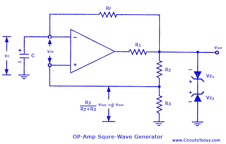
The non-sinusoidal waveform generators are also called relaxation oscillators. The op-amp relaxation oscillator shown in figure is a square wave generator. In general, square waves are relatively easy to produce. Like the UJT relaxation oscillator, the circuit’s frequency of oscillation is dependent on the charge and discharge of a capacitor C through feedback resistor R,. The “heart” of the oscillator is an inverting op-amp comparator
The compa­rator uses positive feedback that increases the gain of the amplifier. In a comparator circuit this offer two advantages. First, the high gain causes the op-amp’s output to switch very quickly from one state to an­other and vice-versa. Second, the use of positive feedback gives the circuit hysteresis. In the op-amp square-wave generator circuit given in figure, the output voltage vout is shunted to ground by two Zener diodes Z1 and Z2 connected back-to-back and is limited to either  VZ 2 or –VZ 1. A fraction of the output is fedback to the non-inverting (+) input terminal. Combination of IL and C acting as a low-pass R-C circuit is used to integrate the output voltage vout and the capacitor voltage vc is applied to the inverting input terminal in place of external signal. The differential input voltage is given as vin = vc - β vout
When vin is positive, vout = – Vz1 and when vin is negative vout = + Vz 2. Consider an instant of time when vin < 0. At this instant vout = + Vz 2 , and the voltage at the non-inverting (+) input terminal is  β Vz 2 , the capacitor C charges exponentially towards Vz 2, with a time constant Rf C. The output voltage remains constant at Vz 2 until vc equal β Vz 2.
When it happens, comparator output reverses to – Vz 1. Now vc changes exponentially towards -Vz1 with  the  same  time  constant  and  again  the  output  makes  a  transition  from -Vz1 to + Vz 2. when vc equals -βVz 1
Let    Vz1 = Vz 2
The time period, T, of the output square wave is determined using the charging and discharging phenomena of the capacitor C. The voltage across the capacitor, vc when it is charging from – B Vz to + Vz is given by
Vc = [1-(1+β)]e-T/2τ
Where τ = RfC
The waveforms of the capacitor voltage vc and output voltage vout (or vz) are shown in figure.
When t = t/2
Vc = +β Vz or + β Vout
Therefore β Vz = Vz [1-(1+β)e-T/2τ]
Or e-T/2τ = 1- β/1+ β
Or T = 2τ loge 1+β/1- β = 2Rf C loge [1+ (2R3/R2)]
Square Wave Generator Waveforms using 741IC
The frequency, f = 1/T , of the square-wave is independent of output voltage Vout. This circuit is also known as free-running or astable multivibrator because it has two quasi-stable states. The output remains in one state for time T1 and then makes an abrupt transition to the second state and re­mains in that state for time T2. The cycle repeats itself after time T = (T1 + T2) where T is the time period of the square-wave.
The op-amp square-wave generator is useful in the frequency range of about 10 Hz -10 kHz. At higher frequencies, the op-amp’s slew rate limits the slope of the output square wave. The symmetry of the output waveform depends on the matching of two Zener diodes Z1 and Z2. The unsymmetrical square-wave (T1 not equal to t2) can be had by using different constants for charging the capacitor C to +Vout and -Vout

Isnin, April 15, 2013

Sabertooth Dual Motor Speed Controllers

Free Electronic/electric Circuit diagram for many electronic project, electrical project and electromachanical.


Sabertooth 2X12 R/C is a dual motor driver specifically optimized for use in radio controlled vehicles. It is suitable for medium powered robots, cars and boats. The Sabertooth 2x12 RC replaces our 2x10 RC controller.


Out of the box, it can supply two DC brushed motors with up to 12A each. Peak currents of 25A are achievable for a few seconds. Overcurrent and thermal protection means you'll never have to worry about killing the driver with accidental stalls or by hooking up too big a motor.


This special R/C edition of our motor driver comes with options for exponential control, autocalibration and built-in mixing. The operating mode is set with the onboard DIP switches so there are no jumpers to lose.


Sabertooth is the first synchronous regenerative motor driver in its class. The regenerative topology means that your batteries get recharged whenever you command your robot to slow down or reverse. Sabertooth also allows you to make very fast stops and reverses - giving your vehicle a quick and nimble edge.


Sabertooth has a built in 5V Switching BEC that can provide power to a microcontroller or R/C receiver and a servo or two. The lithium cutoff mode allows Sabertooth to operate safely with lithium ion and lithium polymer battery packs - the highest energy density batteries available.


Sabertooth's transistors are switched at ultrasonic speeds (32kHz) for silent operation.


1 Amp Switching BEC - Can now power your receiver and multiple servos


12 Amp Continuous/25A Peak Power Rating - A redesigned power stage increases current handling capabilities


Acceleration Ramping - Selectible by DIP switches. Replaces the flip function.


6.0 - 25.0V input
Current handling up to 18V12 amps continuous, 25A Peak per channel
Current handling at 24V10 amps continuous, 12A continuous with airflow, 25A peak per channel
Size2.3" x 1.8" x 0.75"
Weight1.5 oz (43g)
Synchronous regenerative driveyes
Ultra-sonic switching frequencyyes
Thermal and overcurrent protectionyes
Lithium protection modeyes
Here is a great DIP switch wizard that will help you configure your Sabertooth.

Rabu, April 10, 2013

STAGE INTERCOM SYSTEM


Free Electronic/electric Circuit diagram for many electronic project, electrical project and electromachanical.


STAGE INTERCOM SYSTEM


INTRODUCTION


This intercom was built specifically for the school hall where I teach. in the past, walkie talkie's with headsets just didn't work. They were unreliable and not very good quality thus causing problems when needing to communicate backstage or from the lighting desk (where I sit) to the sound desk, spot operators, or video cameras. So a good quality, reliable system that was hard wired was needed. I had some idea of what we needed since we take part in The Global Rock Challenge every year and on some occasions I had directed the lighting for the performances. We had also hired the local theatre to put on 3 day performances where again I had the opportunity to use professional lighting desks and understand how communication occured in the theatre. There is loads of dialogue you never hear!


HALL SETUP

 
Our hall is quite large and can seat 400 audience approx. The layout is shown to the right. There are 9 intercom points at present with more easily added.

Main Hall
Balcony
  • Lighting Desk x 2
  • Sound Desk
  • Spot 1
  • Spot 2

  • Camera1
  • Conductor/Cam2
  • Backstage left
  • Backstage right


The intercoms were designed so that they can be added at will to any part of the link line. The Link is a 2 core 14 strand speaker cable of pretty standard quality but it provides almost a noise free connection.
At first batteries were used but since the current consumption can reach 35mA or more with the LED's, a low voltage power ring was installed alongside the audio Link cable. This was powered by a Science lab 4A supply - no more power supply worries!


CIRCUIT DESCRIPTION  

The circuit diagram below shows the two distinct parts of the circuit. They are based upon standard amplifier designs. The top section is the low signal pre-amplifier for the microphone and the lower section is the power amplifier for the headset. Due to its simplicity, an intercom complete costs less £10 to build.
Note there are many components not mounted on the PCB. Connections to the PCB are denoted by SIL or TB.
PRE-AMP
This amplifier is a standard inverting amplifier based around a 741 op-amp with decoupling capacitors. The gain is set by
-R5/R4 = 1M/10K = 100.
This provides an output around 500-800mV which is fed to the level preset on the PCB to adjust the level of signal placed on the Link. Connection to the Link is via SW2 to enable muting, but audio audio receptions will still be heard from other intercoms.
To enable the amplifier to work on a single voltage supply, a psuedo 0v was created by R2,R3,C1 which gives the amplifier 9 - 4.5 - 0v to operate from.
POWER AMP
This is based around the LM386 IC which provides about 500mW with just 4 components. The volume is set by VR2 which is mounted on the lid.
POWER SUPPLY
This uses a 9v/7.2v PP3 which powers the intercom via a switched 2.1mm DC power socket. The switched contacts inside allow for the battery to be charged through R9 when a supply of 10v or more is pluged in. If you are using a power supply, which is advised, then remove the battery unless it is rechargeable.


ASSEMBLY  
Diagram with lid open showing routing of wires. Thick grey wires are screend cable.


FRONT PANEL
Below is the legend graphics for the front of the case. This was printed onto acetate as a mirror image so the ink was on the underside and was protected by the acetate - genius!


Unfortunately the wiring is a little complex inside but reduced a little by mounting components between switches and LED's. The case used was cheap but not bad looking but since I needed a few of them, cost was a factor. The battery compartment was made from a piece of vacuum forming polystyrene and a bit of foam from the textiles department to stop the battery knocking about. Adhesive PCB posts were used to mount the PCB - quick and simple.


The PCB measures 61mm x 45mm, (2.4" x 1.8"). 4mm holes were drilled for the PCB posts. SIL connectors were not used to reduce cost and save the hassle of crimping connectors. A PCB terminal block was used for the power supply however - their ease is worth the cost.


फ्लेअसे गीवे यौर कॉमेण . टQ  


Ahad, Mac 03, 2013

60W Amplifier


Low-cut and Bass controls
Output power: 40W on 8 Ohm and 60W on 4 Ohm loads
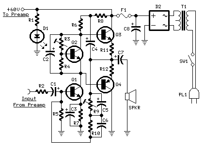
Amplifier circuit diagram:

Amplifier parts:
R1 6K8 1W Resistor
R2,R4 470R 1/4W Resistors
R3 2K 1/2W Trimmer Cermet
R5,R6 4K7 1/2W Resistors
R7 220R 1/2W Resistor
R8 2K2 1/2W Resistor
R9 50K 1/2W Trimmer Cermet
R10 68K 1/4W Resistor
R11,R12 R47 4W Wirewound Resistors
C1,C2,C4,C5 47µF 63V Electrolytic Capacitors
C3 100µF 25V Electrolytic Capacitor
C6 33pF 63V Ceramic Capacitor
C7 1000µF 50V Electrolytic Capacitor
C8 2200µF 63V Electrolytic Capacitor (See Notes)
D1 LED Any type and color
D2 Diode bridge 200V 6A
Q1,Q2 BD139 80V 1.5A NPN Transistors
Q3 MJ11016 120V 30A NPN Darlington Transistor (See Notes)
Q4 MJ11015 120V 30A PNP Darlington Transistor (See Notes)
SW1 SPST Mains switch
F1 4A Fuse with socket
T1 220V Primary, 48-50V Secondary 75 to 150VA Mains transformer
PL1 Male Mains plug
SPKR One or more speakers wired in series or in parallel. Total resulting impedance: 8 or 4 Ohm. Minimum power handling: 75W
Preamplifier circuit diagram:

Preamplifier parts:
P1 10K Linear Potentiometer
P2 10K Log. Potentiometer
R1,R2 68K 1/4W Resistors
R3 680K 1/4W Resistor
R4 220K 1/4W Resistor
R5 33K 1/4W Resistor
R6 2K2 1/4W Resistor
R7 5K6 1/4W Resistor
R8,R18 330R 1/4W Resistors
R9 47K 1/4W Resistor
R10 18K 1/4W Resistor
R11 4K7 1/4W Resistor
R12 1K 1/4W Resistor
R13 1K5 1/4W Resistor
R14,R15,R16 100K 1/4W Resistors
R17 10K 1/4W Resistor
C1,C4,C8,C9,C10 10µF 63V Electrolytic Capacitors
C2 47µF 63V Electrolytic Capacitor
C3 47pF 63V Ceramic Capacitor
C5 220nF 63V Polyester Capacitor
C6 470nF 63V Polyester Capacitor
C7 100nF 63V Polyester Capacitor
C11 220µF 63V Electrolytic Capacitor
Q1,Q3 BC546 65V 100mA NPN Transistors
Q2 BC556 65V 100mA PNP Transistor
J1,J2 6.3mm. Mono Jack sockets
SW1 SPST Switch
Circuit description:
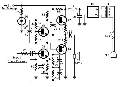
This design adopts a well established circuit topology for the power amplifier, using a single-rail supply of about 60V and capacitor-coupling for the speaker(s). The advantages for a guitar amplifier are the very simple circuitry, even for comparatively high power outputs, and a certain built-in degree of loudspeaker protection, due to capacitor C8, preventing the voltage supply to be conveyed into loudspeakers in case of output transistors' failure.
The preamp is powered by the same 60V rails as the power amplifier, allowing to implement a two-transistors gain-block capable of delivering about 20V RMS output. This provides a very high input overload capability.
Technical data:
Sensitivity:
70mV input for 40W 8 Ohm output
63mV input for 60W 4 Ohm output
Frequency response:
50Hz to 20KHz -0.5dB; -1.5dB @ 40Hz; -3.5dB @ 30Hz
Total harmonic distortion @ 1KHz and 8 Ohm load:
Below 0.1% up to 10W; 0.2% @ 30W
Total harmonic distortion @ 10KHz and 8 Ohm load:
Below 0.15% up to 10W; 0.3% @ 30W
Total harmonic distortion @ 1KHz and 4 Ohm load:
Below 0.18% up to 10W; 0.4% @ 60W
Total harmonic distortion @ 10KHz and 4 Ohm load:
Below 0.3% up to 10W; 0.6% @ 60W
Bass control:
Fully clockwise = +13.7dB @ 100Hz; -23dB @ 10KHz
Center position = -4.5dB @ 100Hz
Fully counterclockwise = -12.5dB @ 100Hz; +0.7dB @ 1KHz and 10KHz
Low-cut switch:
-1.5dB @ 300Hz; -2.5dB @ 200Hz; -4.4dB @ 100Hz; -10dB @ 50Hz
Notes:
The value listed for C8 is the minimum suggested value. A 3300µF capacitor or two 2200µF capacitors wired in parallel would be a better choice.
The Darlington transistor types listed could be too oversized for such a design. You can substitute them with MJ11014 (Q3) and MJ11013 (Q4) or TIP142 (Q3) and TIP147 (Q4).
T1 transformer can be also a 24 + 24V or 25 + 25V type (i.e. 48V or 50V center tapped). Obviously, the center-tap must be left unconnected.
SW1 switch inserts the Low-cut feature when open.
In all cases where Darlington transistors are used as the output devices it is essential that the sensing transistor (Q2) should be in as close thermal contact with the output transistors as possible. Therefore a TO126-case transistor type was chosen for easy bolting on the heatsink, very close to the output pair.
R9 must be trimmed in order to measure about half the voltage supply from the positive lead of C7 and ground. A better setting can be done using an oscilloscope, in order to obtain a symmetrical clipping of the output waveform at maximum output power.
To set quiescent current, remove temporarily the Fuse F1 and insert the probes of an Avo-meter in the two leads of the fuse holder.
Set the volume control to the minimum and Trimmer R3 to its minimum resistance.
Power-on the circuit and adjust R3 to read a current drawing of about 30 to 35mA.
Wait about 15 minutes, watch if the current is varying and readjust if necessary.

50W Amplifier

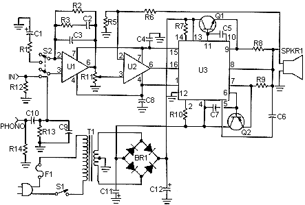
This is a handy, easy to build general purpose 50 watt amp. The amp has an input for a radio, TV, stereo or other line level device. It also has a phono input for a record player, guitar, microphone or other un-amplified source. With the addition of a low pass filter at the input, it makes a great amp for a small subwoofer.
circuit diagram

parts
R1 200 Ohm 1/4 W Resistor
R2 200K 1/4 W Resistor
R3 30K 1/4 W Resistor
R5 1K 1/4 W Resistor
R6 5K 1/4 W Resistor
R7,R10 1 Meg (5%) 1/2 W Resistor
R8,R9 0.4 Ohm 5 W Resistor
R11 10K Pot
R12,R13 51K 1/4 W Resistor
R14 47K 1/4 W Resistor
C1 100uF 35V Electrolytic Capacitor
C2 0.011uF Capacitor
C3 3750pF Capacitor
C4,C6 1000pF Capacitor
C5,C7,C8 0.001uF Capacitor
C9 50pF Capacitor
C10 0.3uF Capacitor
C11,C12 10,000uF 50V Electrolytic Capacitor
U1,U2 741 Op Amp
U3 ICL8063 Audio Amp Transister Driver thingy
Q1 2N3055 NPN Power Transistor
Q2 2N3791 PNP Power Transistor
notes
1. I know I skipped R4. That is not a problem :-)
2. Distortion is less than 0.1% up to 100HZ and increases to about 1% at 20kHz.
3. I haven't been able to find anyone who sells a suitable T1. You can always use two 24V 5A units in series. If you are building two amps (for stereo), then I would suggest using an old microwave transformer and rewinding it.
4. Q1 and Q2 will require heatsinks.

100W Amplifier


Circuit Description:
This is a 100 watt basic power amp that was designed to be (relatively) easy to build at a reasonable cost. It has better performance (read: musical quality) than the standard STK module amps that are used in practically every mass market stereo receiver manufactured today. When I originally built this thing, it was because I needed a 100 WPC amp and didn't want to spend any money. So I designed around parts I had in the shop.
The design is pretty much a standard one, and I'm sure there are commercial units out there that are similar. To my knowlwdge, it is not an exact copy of any commercial unit, nor am I aware of any patents on the topology. To experienced builders: I realize that many improvements and refinements can be made, but the idea was to keep it simple, and should be do-able by anyone who can make a circuit board and has the patience not to do a sloppy job.
The input stage is an LF351 op amp which provides most of the open loop gain as well as stabilizes the quiescent dc voltage. This feeds a level shift stage which references the voltage swing to the (-) rail. The transconductance stage is a darlington, to improve high-frerqency linearity. The 2SC2344 by itself has a rather large collector-base capacitance which is voltage dependent. The MPSA42 presents this with a low-z and has a C(ob) of only a few pf that is effectively swamped by the 33pF pole-splitting cap. The stage is supplied by the 2SA1011 active load (current source) which is about 20 ma. The current to the stage is limited by the 2N3094 to about 70 ma under worst case.
The output is a full complementary darlington with paralleled outputs. Although you could "get away with" only one if only 8 ohm easy-to-drive loads are used, this is not recommended. The use of parallel devices increases the ability to drive reactive loads (which can pull a significant current while the voltage waveform crosses zero and puts a high voltage and a high curent across the transistor simultaneously), gives the amp a higher damping factor, and reduces the maximum current each transistor has to supply to peaks (remember, the gain of a power transistor drops as the current increases).
Compensation is two-pole and one zero. The op-amp's pole and the pole generated by the 33pf cap and the 470 ohm bias resistor of the MPSA42 dominate. (the 33pF gets multiplied by the stage gain.) The 22 pf feedback capacitor provides lead compensation, and is taken from the output of the tranconductance stage rather than the output itself. In this way, the phase lag introduced by the output transistors is not seen by the high-frequency feedback. This intorduces a closed-loop pole which limits the high-frequency response. The two compensation capacitors must be type 1 creamic (NPO) or silver mica - with ZERO voltage coefficient.
The amp was designed to run 2 channels off a +/- 55 volt unregulated supply, reducing to +/- 48 volts under full load. It used a 40-0-40 volt, 5 amp toroid transformer, a bridge rectifier, and 10,000 uf of filter cap per side. If a standard EI transformer is used, a 6-amp rated unit should be used. With this power supply, it produces 100 watts continuous, both channels driven into 8 ohms resistive with no clipping. Dynamic headroom is about a db and a half. For more headroom, unloaded voltages to +/- 62 volts can be used with no circuit modification.
By the way, the schematic is in Postscript.
Limitations:
With no modifications the amp will drive 4-ohm speaker systems with no current limiting. The short-circuit current limit is set to about 4.5 amps peak, which will handle conventional speaker loads.(It will, of course, produce higher peak currents as the output voltage swing approaches the rail.) If you are going to be running some of those high-end speakers with impedance minima of half an ohm, or that stay reactive throughout most of the audio band ( ie, 0.5 +j3.2 ohms) you will probably already own a better amp than this. If the higher-power Motorola power transistors are used, it will drive a 2-ohm resistive load without problems (except heat).
I have never heard any slew-induced distortion on this amp with a CD player's band-limited (22KHz) signal. I suppose that real high-end freaks could pick it to pieces by hitting it with a TTL square wave mixed with a 19KHz stereo pilot tone and crank it up. I guarantee that there will be spurs all over the spectrum, but who listens to that?
Possible Modifications: (What if I want mo' power???)
The Toshiba output transistors (2SD424/2SB554 pair) shoud not be used with supply voltages above +/-60 volts. If you plan on cranking it up, use more in parallel or use the 250 watt Motorola pairs (MJ15024/MJ15025). If very low impedances are expected, raise the bias in the transconductance stage to give more base drive to the output darlingtons or add another current gain stage. Higher-Beta (and faster) power transistors can't handle reactive loads worth a crap. Don't substitute high-fT parts unless you are sure they have adequate second-breakdown capability.
The NE5532 op-amp can be used in the input stage. If more than one are used off the +/-15 volt shunt regulators (balanced ins, anti-slew Bessel filters, etc.) the 2.7K dropping resistors may need to be reduced to say, 1.8K ohm to maintain regulation. The 2.7K resistors will allow up to 4 LF351 type op amps off the regulator (I used a quad 347 for balanced inputs to avoid hum in a DJ setup).
Construction tips:
The output transistors and thermal compensator (2SC1567) will need to be mounted on a common heat sink - a finned unit measuring 5 in. high by 8 in. wide with 1.25 in fins should do nicely for one channel. (They look nice if you make the sides of the case out of them). Most normal applications won't require more cooling than this. The reason the 2SC1567 was chosen for the output bias regulator is because it is fully insulated - the ECG version will require additional mounting hardware. TO-3 hardware for the outputs is cheap and easy to get.
The driver transistors and voltage amps (2SC3344/2SA1011 pairs) will all require heatsinking as well. Individual TO-220 heat sinks on the circuit board will suffice - the voltage amps dissipate about 1.4 watts each. A common piece of 1/8 in. thick 1 in. wide X 4in. long angle aluminum will suffice for all 4 on each channel, but bear in mind that it must be oriented to take advantage of natural convection, and the transistors must be insualted.
Keep the imput grounds separate from everything else, and return them at ONE point. Failure to do so WILL result in high distortion (5% or so), or even oscillation.
The output stage bias should be set to about 25 milliamps in the output transistors. This value takes a while to stabilize, and you may have to monitor it over an hour or so during initial setup. To measure it, measure the voltage across the emitter resistor and use Ohm's law. This way, you can check the current sharing in the parallel output transistors at the same time and change them if there is a serious discrepancy. With parts of the same date code, they should not be off by more than 10% after it has warmed up. Higher output stage biases can be used, but it takes more care in setting it. If you want an idle current of more than 50 milliamps per side, increase the value of the emitter resistors.
Initial Checkout:
DO NOT just plug something like this in! A seemingly insignificant error can set your house on fire! (As well as blow out $30 worth of transistors in a microsecond.) A variac will work in theory, but the amp may latch to the rail if the supply drops too low. I suggest the use of a ballast resistor - a 60 to 100 watt light bulb in series with the AC mains. You get a bright flash when the caps charge, and then it goes (almost) out as the idling supply current reaches its nominal low value. The amplifier will then work normally at low volumes. If the amp draws too much current for whatever reason, the lightbulb will glow brightly, increase resistance, and limit the power to the circuit. Usually, there will either be a mis-wire (use your DMM) or oscillation (will show up on a scope or RF power measuring device). If the bulb goes dim-bright-dim-bright... then the amp is marginally stable and the grounding layout should be checked. Compensation capacitor values may need to be adjusted if any significant changes were made. Mine is stable the way it is.
Additional Notes:
The schematic is in postcript, so it should just be able to be printed out. The emitters of the transistors are labelled by an "e". I was too lazy to put arrows on the transistor symbols - and I've been using it that way for over a year now.
Trouble finding parts? MCM (1-800-543-4330) has all the transistors. Total cost for a stereo version should be between $150 and $250, depending on what kind of bargains you can find on the case, transformer, and heatsinks. If you have to pay "list" for everything, it will likely cost about $1000 to build.
The information included herin is provided as-is, with no warranties express or implied. No resposibility on the part of the author is assumed for the technical accuracy of the information given herein or the use or mis-use of said information.
The equipment described in this article was designed, fabricated, and tested on my own personal time using my own personal resources.


Click HERE to get the postscript circuit diagram.
Click HERE to get the pdf circuit diagram.

10W Mini Audio Amplifier

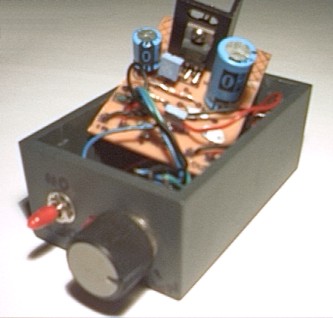
finished device

Componets Layout

PCB

Componets List
R1 : 6 Ohm
R2 : 220 Ohm
R3 : nothing
R4 : 10 KOhm pontesiometer
C1 : 2200 uF / 25V
C2 : 470 uF / 16V
C3 : 470 nF / 63V
C4 : 100 nF
C5 : nothing
C6 : nothing
IC1 : TDA 2003

Subwoofer Power Amplifier


he acoustic spectrum is extended by very low frequencies 20Iz and reaches as the 20000Iz in high frequencies. In the low frequencies is degraded the sense of direction. This reason us leads to the utilization speaker for the attribution of very low frequencies. The manufacture that to you we propose distinguishes these frequencies, in order to him we lead to the corresponding amplifier. The acoustic filters are met in various points in the sound systems. The knownest application they are the filters baxandal for regulating tone low and high frequencies and filters crossover where the acoustic region is separated in subareas, in order to it leads the corresponding loudspeakers. The application that to you we propose is a simple filter of region that limits the acoustic region (20-20000Hz) in the region 20-100Hz.
With the manufacture that to you we propose you can make a active filter in order to you lead a loudspeaker of very low frequencies. With this you will place one bigger speaker between the HIFI speakers of you. In order to you have a complete picture of sound you will need also the corresponding amplifier. In the entry of circuit you will connect the two exits of preamplifier or the exit of line of some preamplifier. The circuit of manufacture allocates a exit in order to is led means of circuit of force subwoofer. If for some reason you do not have space in order to you place the third speaker in space of hearing, then you can select smaller speaker. The output will depend from the type of music that you hear. If in deed you have space, then after you make a filter and remain thanked, you can him recommend in your friends or still make other same for your friends.


In the form it appears the theoretical circuit of filter. In first glance we see three different circuits that are mainly manufactured round two operational amplifiers. This circuits constitute mixed, amplifier with variable aid and a variable filter. The manufacture end needs a circuit of catering with operational tendency of catering equal with ±12. the operational amplifiers that constitute the active elements for this circuits of are double operational type as the TL082 and NE5532. The operational these amplifiers belong in a family provided with transistor of effect of field IFET in their entries. Each member of family allocates in their circuit bipolar transistor and effect of field. This circuits can function in his high tendency, because that they use transistor of high tendency. Also they have high honor of rhythm of elevation (slew rate), low current of polarization for the entries and are influenced little by the temperature. The operational these amplifiers have breadth of area unity gain bandwidth 3MHz. A other important element for their choice is the big reject of noise, when this exists in the line of catering.
The price of reject is bigger than 80dB, their consumption is small, from 11 until 3 mA. They are internally sold in nutshell with eight pins and allocate two operational amplifiers, In the same line in nutshell 14 pins they incorporate four operational, In the trade they are sold with code TL074, TL084 and TL064, In nutshell with eight pins they are sold operational amplifiers TL061 TL071 kajTL081. In the manufacture we used the TL082 that has two operational. First operational from the TL082 it works as amplifier and mixed for the two channels, In his negative entry he exists one small mixed with two resistances. A potentiometer in this rung determines the aid of circuit. In the point this left winger and the right channel of preamplifier they are added means of two resistances. En continuity the operational strengthens signal with aid made dependent from the price that has the potentiometer.
The place of runner is proportional with the aid of circuit. The second operational amplifier is the filter of manufacture. The filter of is acoustic frequency of second class and he is made with the materials that are round the operational amplifier. The filter of is low passage with variable frequency of cutting off. This frequency can be altered and take prices from very low frequency the 30Hz or still exceed 150Hz. The frequency of cutting off of filter depends from the prices that have the elements of circuit. Altering the values of elements we can have frequency of cutting off 150Iz, 130Iz, J00Iz, 7Ïz, 6Íz even 3Íz, this prices they can be achieved with the simple rotation of double potentiometer. The circuit of filter has been made around one operational' that it has completed TL082 that is double operational amplifier. In the exit of filter we will link the plug of expense where is connected the amplifier. In the exit of circuit is presented, the limited as for the breadth of frequencies, signal that we apply in the entry of circuit.
Manufacture
Parts
R1 = 39 Kohm
R2 = 39 Kohm
R3 = 47 Kohm
R4 = 10 Ohm
R5 = 22 Kohm
R6 = 4,7 Kohm
R7 = 22 Kohm
R8 = 4,7 Kohm
R9 = 10 Ohm
R10 = 220 Ohm
C1 = 39 pF
C2 = 0.1 uF
C3 = 0.1 uF
C4 = 0.2 uF
C5 = 0.4 uF
C6 = 0.1 uF
C7 = 0.1 uF
IC1 = TL064
In order to you make the manufacture you will need printed that appears in the form. In this you will place the materials according to the following form. The materials are enough also easy can become certain errors. With few attention however you can him avoid. If they are presented difference malfunctions, you check carefully the circuit. The circuit, as we said, is filter and it should they are used materially good precision and quality, particularly for the capacitors. The capacitors of filters will have tolerance 5%. Of course, the manufacture will also work with material of lower quality, the trial of manufacture can become with acoustic signal of generator We apply the generator in the entry of manufacture and we measure with a voltmeter the tendency in the exit of filter. If we alter the potentiometer and are altered the tendency, then all have well.

2N3055 Power Amplifier


Simple and low cost. The optimal supply voltage is around 50V, but this amp work from 30 to 60V. The maximal input voltage is around 0.8 - 1V. As you can see, in this design the components have a big tolerance, so you can build it almost of the components, which you find at home. The and transistors can be any NPN type power transistor, but do not use Darlington types... The output power is around 60W.
Some comments:
- capacitor C1 regulates the low frequencies (bass), as the capacitance grows, the low frequncies are getting louder.
- capacitor C2 regulates the higher frequencies (treble), as the capacitance grows, the higher frequencies are getting quiter.
- this is a class B amplifier, this means, that a current must flow through the end transistors, even if there is no signal on the input. This current can be regulated with the 500ohm; trimmer resistor. As this current incrases, the sound of the amplifier gets better, but the end transistors are more heating. But if this current decrases, the transistors are not heating so much, but the sound gets worse...

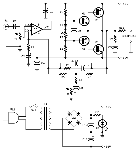
20Wpp Audio Amplifier with Bass


Audio circuit diagram

Parts:
P1 22K Log.Potentiometer (Dual-gang for stereo)
P2 100K Log.Potentiometer (Dual-gang for stereo)
R1 820R 1/4W Resistor
R2,R4,R8 4K7 1/4W Resistors
R3 500R 1/2W Trimmer Cermet
R5 82K 1/4W Resistor
R6,R7 47K 1/4W Resistors
R9 10R 1/2W Resistor
R10 R22 4W Resistor (wirewound)
C1,C8 470nF 63V Polyester Capacitor
C2,C5 100uF 25V Electrolytic Capacitors
C3,C4 470uF 25V Electrolytic Capacitors
C6 47pF 63V Ceramic or Polystyrene Capacitor
C7 10nF 63V Polyester Capacitor
C9 100nF 63V Polyester Capacitor
D1 1N4148 75V 150mA Diode

IC1 NE5532 Low noise Dual Op-amp

Q1 BC547B 45V 100mA NPN Transistor
Q2 BC557B 45V 100mA PNP Transistor
Q3 TIP42A 60V 6A PNP Transistor
Q4 TIP41A 60V 6A NPN Transistor
J1 RCA audio input socket


Power supply parts:
R11 1K5 1/4W Resistor
C10,C11 4700uF 25V Electrolytic Capacitors
D2 100V 4A Diode bridge
D3 5mm. Red LED
T1 220V Primary, 12 + 12V Secondary 24-30VA Mains transformer
PL1 Male Mains plug
SW1 SPST Mains switch
Comments:
This design is based on the 18 Watt Audio Amplifier, and was developed mainly to satisfy the requests of correspondents unable to locate the TLE2141C chip. It uses the widespread NE5532 Dual IC but, obviously, its power output will be comprised in the 9.5 - 11.5W range, as the supply rails cannot exceed ±18V.
As amplifiers of this kind are frequently used to drive small loudspeaker cabinets, the bass frequency range is rather sacrificed. Therefore a bass-boost control was inserted in the feedback loop of the amplifier, in order to overcome this problem without quality losses. The bass lift curve can reach a maximum of +16.4dB @ 50Hz. In any case, even when the bass control is rotated fully counterclockwise, the amplifier frequency response shows a gentle raising curve: +0.8dB @ 400Hz, +4.7dB @ 100Hz and +6dB @ 50Hz (referred to 1KHz).
Notes:
Can be directly connected to CD players, tuners and tape recorders.
Schematic shows left channel only, but C3, C4, IC1 and the power supply are common to both channels.
Numbers in parentheses show IC1 right channel pin connections.
A log type for P2 ensures a more linear regulation of bass-boost.
Don't exceed 18 + 18V supply.
Q3 and Q4 must be mounted on heatsink.
D1 must be in thermal contact with Q1.
Quiescent current (best measured with an Avo-meter in series with Q3 Emitter) is not critical.
Set the volume control to the minimum and R3 to its minimum resistance.
Power-on the circuit and adjust R3 to read a current drawing of about 20 to 25mA.
Wait about 15 minutes, watch if the current is varying and readjust if necessary.
A correct grounding is very important to eliminate hum and ground loops. Connect in the same point the ground sides of J1, P1, C2, C3 &C4. Connect C9 at the output ground.
Then connect separately the input and output grounds at the power supply ground.
Technical data:
Output power: 10 Watt RMS @ 8 Ohm (1KHz sinewave)
Sensitivity: 115 to 180mV input for 10W output (depending on P2 control position)
Frequency response: See Comments above
Total harmonic distortion @ 1KHz: 0.1W 0.009% 1W 0.004% 10W 0.005%
Total harmonic distortion @ 100Hz: 0.1W 0.009% 1W 0.007% 10W 0.012%
Total harmonic distortion @10KHz: 0.1W 0.056% 1W 0.01% 10W 0.018%
Total harmonic distortion @ 100Hz and full boost: 1W 0.015% 10W 0.03%
Max. bass-boost referred to 1KHz: 400Hz = +5dB; 200Hz = +7.3dB; 100Hz = +12dB; 50Hz = +16.4dB; 30Hz = +13.3dB
Unconditionally stable on capacitive loads

60W Guitar Amplifier


Bass, Treble, Harmonic modifier and Brightness controls

Output power: 40W on 8 Ohm and 60W on 4 Ohm loads
Amplifier circuit diagram:

Amplifier parts:
R1 6K8 1W Resistor
R2,R4 470R 1/4W Resistors
R3 2K 1/2W Trimmer Cermet
R5,R6 4K7 1/2W Resistors
R7 220R 1/2W Resistor
R8 2K2 1/2W Resistor
R9 50K 1/2W Trimmer Cermet
R10 68K 1/4W Resistor
R11,R12 R47 4W Wirewound Resistors
C1,C2,C4,C5 47µF 63V Electrolytic Capacitors
C3 100µF 25V Electrolytic Capacitor
C6 33pF 63V Ceramic Capacitor
C7 1000µF 50V Electrolytic Capacitor
C8 2200µF 63V Electrolytic Capacitor (See Notes)
D1 LED Any type and color
D2 Diode bridge 200V 6A
Q1,Q2 BD139 80V 1.5A NPN Transistors
Q3 MJ11016 120V 30A NPN Darlington Transistor (See Notes)
Q4 MJ11015 120V 30A PNP Darlington Transistor (See Notes)
SW1 SPST Mains switch
F1 4A Fuse with socket
T1 220V Primary, 48-50V Secondary 75 to 150VA Mains transformer (See Notes)
PL1 Male Mains plug
SPKR One or more speakers wired in series or in parallel. Total resulting impedance: 8 or 4 Ohm. Minimum power handling: 75W
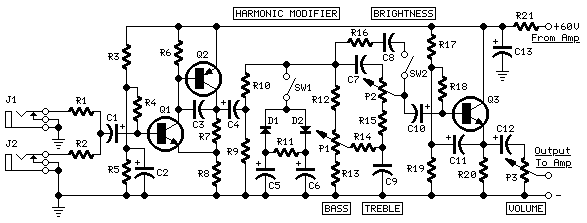
Preamplifier circuit diagram:

Preamplifier parts:
P1,P2 10K Linear Potentiometers
P3 10K Log. Potentiometer
R1,R2 68K 1/4W Resistors
R3 680K 1/4W Resistor
R4 220K 1/4W Resistor
R5 33K 1/4W Resistor
R6,R16 2K2 1/4W Resistors
R7 5K6 1/4W Resistor
R8,R21 330R 1/4W Resistors
R9 47K 1/4W Resistor
R10 470R 1/4W Resistor
R11 4K7 1/4W Resistor
R12,R20 10K 1/4W Resistors
R13 100R 1/4W Resistor
R14,R15 47R 1/4W Resistors
R17,R18,R19 100K 1/4W Resistors
C1,C4,C5,C6 10µF 63V Electrolytic Capacitors
C2 47µF 63V Electrolytic Capacitor
C3 47pF 63V Ceramic Capacitor
C7 15nF 63V Polyester Capacitor
C8 22nF 63V Polyester Capacitor
C9 470nF 63V Polyester Capacitor
C10,C11,C12 10µF 63V Electrolytic Capacitors
C13 220µF 63V Electrolytic Capacitor
D1,D2 BAT46 100V 150mA Schottky-barrier Diodes (see Notes)
Q1,Q3 BC546 65V 100mA NPN Transistors
Q2 BC556 65V 100mA PNP Transistor
J1,J2 6.3mm. Mono Jack sockets
SW1,SW2 SPST Switches
Circuit description:
This design adopts a well established circuit topology for the power amplifier, using a single-rail supply of about 60V and capacitor-coupling for the speaker(s). The advantages for a guitar amplifier are the very simple circuitry, even for comparatively high power outputs, and a certain built-in degree of loudspeaker protection, due to capacitor C8, preventing the voltage supply to be conveyed into loudspeakers in case of output transistors' failure.
The preamp is powered by the same 60V rails as the power amplifier, allowing to implement a two-transistors gain-block capable of delivering about 20V RMS output. This provides a very high input overload capability.
Technical data:
Sensitivity:
35mV input for 40W 8 Ohm output
42mV input for 60W 4 Ohm output
Frequency response:
50Hz to 20KHz -0.5dB; -1.5dB @ 40Hz; -3.5dB @ 30Hz
Total harmonic distortion @ 1KHz and 8 Ohm load:
Below 0.1% up to 10W; 0.2% @ 30W
Total harmonic distortion @ 10KHz and 8 Ohm load:
Below 0.15% up to 10W; 0.3% @ 30W
Total harmonic distortion @ 1KHz and 4 Ohm load:
Below 0.18% up to 10W; 0.4% @ 60W
Total harmonic distortion @ 10KHz and 4 Ohm load:
Below 0.3% up to 10W; 0.6% @ 60W
Treble control:
+9 / -16dB @ 1KHz; +12 / -24dB @ 10KHz
Brightness control:
+6.5dB @ 500Hz; +7dB @ 1KHz; +8.5dB @ 10KHz
Bass control:
-17.5dB @ 100Hz; -26dB @ 50Hz; -28dB @ 40Hz
Notes:
The value listed for C8 is the minimum suggested value. A 3300µF capacitor or two 2200µF capacitors wired in parallel would be a better choice.
The Darlington transistor types listed could be too over sized for such a design. You can substitute them with MJ11014 (Q3) and MJ11013 (Q4) or TIP142 (Q3) and TIP147 (Q4).
T1 transformer can be also a 24 + 24V or 25 + 25V type (i.e. 48V or 50V center tapped). Obviously, the center-tap must be left unconnected.
D1 and D2 can be any Schottky-barrier diode types. With these devices, the harmonic modifier operation will be hard. Using for D1 and D2 two common 1N4148 silicon diodes, the harmonic modifier operation will be softer.
In all cases where Darlington transistors are used as the output devices it is essential that the sensing transistor (Q2) should be in as close thermal contact with the output transistors as possible. Therefore a TO126-case transistor type was chosen for easy bolting on the heatsink, very close to the output pair.
R9 must be trimmed in order to measure about half the voltage supply from the positive lead of C7 and ground. A better setting can be done using an oscilloscope, in order to obtain a symmetrical clipping of the output waveform at maximum output power.
To set quiescent current, remove temporarily the Fuse F1 and insert the probes of an Avo-meter in the two leads of the fuse holder.
Set the volume control to the minimum and Trimmer R3 to its minimum resistance.
Power-on the circuit and adjust R3 to read a current drawing of about 30 to 35mA.
Wait about 15 minutes, watch if the current is varying and readjust if necessary.

Popular Project

Another Project Blog

Project From Diff Blogger

Links

How to Find the other Websites of a Person?


DomainTools

Whois Source Logo


BetterWhois.com: Search ALL Domain Registrars

Webcams.travel - The Webcam Community - Home